
User guide
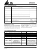
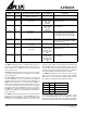


Page 2 Voice Recording & Playback Device
Revision 2.1
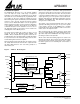
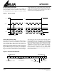
Functional Description
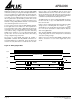
The EXTCLK pin allows the use of an external sampling
clock. This input can accept a wide range of frequencies
dependin
g on the divider ratio programmed into the divider
that follows the clock. Alternativel
y, the programmable inter-
nal oscillator can be used to suppl
y the sampling clock. The
Mux followin
g both signals automatically selects the EXTCLK
si
gnal if a clock is present, otherwise the internal oscillator
source is chosen. Detailed information on how to pro
gram the
divider and internal oscillator can be found in the explanation
of the
PWRUP
command, which appears in the
OpCode
Command Description
section. Guidance on how to choose
the appropriate sample clock fre
quency can be found in the
Sampling Rate & Voice Quality
section.
The audio si
gnal containing the content you wish to record
should be fed into the differential inputs ANAIN-, and
ANAIN+. After pre-amplification the si
gnal is routed into the
anti-aliasin
g filter. The anti-aliasing filter automatically adapts
its response based on the sample rate bein
g used. No exter-
nal anti-aliasin
g filter is therefore required.
After passin
g through the anti-alias filter, the signal is fed into
the sample and hold circuit which works in con
junction with
the Analo
g Write Circuit to store each analog sample in a
flash memor
y cell.
When a read operation is desired the Analog Read Circuit
extracts the analo
g data from the memory array and feeds
the si
gnal to the Internal Low Pass Filter. The low pass filter
converts the individual samples into a continuous output. The
output si
gnal then goes to the squelch control circuit and di-
fferential output driver. The differential output driver feeds the
ANAOUT+ and ANAOUT- pins. Both differential output pins
swin
g around a 1.23V potential.
The s
quelch control circuit automatically reduces the output
si
gnal by 6 dB during quiet passages. A copy of the squelch
control si
gnal is present on the SQLOUT pin to facilitate
reducin
g gain in the external amplifier as well. For more infor-
mation, refer to the
Squelch
section.
After passin
g through the squelch circuit the output signal
goes to the output amplifier. The output amplifier drives a sin-
gle ended output on the AUDOUT pin. The single ended out-
put swin
gs around a 1.23V potential.
All SPI control and hand shakin
g signals are routed to the
Master Control Circuit. This circuit decodes all the SPI si
gnals
and
generates all the internal control signals. It also contains
the status re
gister used for examining the current status of
the APR6008 .
Figure 2 APR6008 Block Diagram
SAC
Low Pass
Master Control Circuit
Amp
SCLK
/CS
DI
DO
/INT
/RESET
AUDOUT
/SQLOUT
Squelch
Amp
ANAOUT+
ANAOUT-
/BUSY
SQLCAP
Row Decoder
Column Decoder
Column Address
Row
Address
Single Analog
Memory Cell
1.92 Mcell Memory Array
Write Circuit
Low Pass
Read Circuit
Analog input/output
to Memory array
Pre-
Amp
ANAIN+
ANAIN-
Programmable Internal
Oscillator
Mux
EXTCLK
Programmable
Divider
APR6008