
Owner's manual


AC Electrical Characteristics (Continued)
Note 1: Absolute Maximum Ratings indicate limits beyond which damage to the device may occur. Operating Ratings indicate conditions for which the device is
functional, but do not guarantee specific performance limits. For guaranteed specifications and test conditions, see the Electrical Characteristics. The guaranteed
specifications apply only for the test conditions listed. Some performance characteristics may degrade when the device is not operated under the listed test
conditions.
Note 2: All voltages are measured with respect to GND, unless otherwise specified.
Note 3: When the input voltage (V
IN
) at any pin exceeds the power supplies (V
IN
k
GND or V
IN
l
V
A
a
or V
D
a
), the current at that pin should be limited to 30 mA.
The 120 mA maximum package input current rating limits the number of pins that can safely exceed the power supplies with an input current of 30 mA to four.
Note 4: The maximum power dissipation must be derated at elevated temperatures and is dictated by T
J
max, i
JA
and the ambient temperature, T
A
. The maximum
allowable power dissipation at any temperature is P
D
e
(T
J
max
b
T
A
)/i
JA
or the number given in the Absolute Maximum Ratings, whichever is lower. For this
device, T
J
max
e
150
§
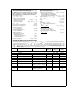
C. The typical thermal resistance (H
JA
) of these parts when board mounted follow:
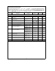
Thermal
Part Number Resistance
i
JA
ADC12130CIN 53
§
C/W
ADC12130CIWM 70
§
C/W
ADC12132CIMSA 134
§
C/W
ADC12138CIN 40
§
C/W
ADC12138CIWM 50
§
C/W
ADC12138CIMSA 125
§
C/W
Note 5: The human body model is a 100 pF capacitor discharged through a 1.5 kX resistor into each pin.
Note 6: See AN450 ‘‘Surface Mounting Methods and Their Effect on Product Reliability’’ or the section titled ‘‘Surface Mount’’ found in any post 1986 National
Semiconductor Linear Data Book for other methods of soldering surface mount devices.
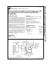
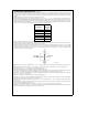
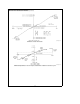
Note 7: Two on-chip diodes are tied to each analog input through a series resistor as shown below. Input voltage magnitude up to 5V above V
A
a
or 5V below GND
will not damage this device. However, errors in the A/D conversion can occur (if these diodes are forward biased by more than 50 mV) if the input voltage
magnitude of selected or unselected analog input go above V
A
a
or below GND by more than 50 mV. As an example, if V
A
a
is 4.5 V
DC
, full-scale input voltage
must be
s
4.55 V
DC
to ensure accurate conversions.
TL/H/12079–4
Note 8: To guarantee accuracy, it is required that the V
A
a
and V
D
a
be connected together to the same power supply with separate bypass capacitors at each V
a
pin.
Note 9: With the test condition for V
REF
(V
REF
a
b
V
REF
b
) given as
a
4.096V, the 12-bit LSB is 1.0 mV. For V
REF
e
2.5V, the 12-bit LSB is 610 mV.
Note 10: Typicals are at T
J
e
T
A
e
25
§
C and represent most likely parametric norm.
Note 11: Tested limits are guaranteed to National’s AOQL (Average Outgoing Quality Level).
Note 12: Positive integral linearity error is defined as the deviation of the analog value, expressed in LSBs, from the straight line that passes through positive full-
scale and zero. For negative integral linearity error, the straight line passes through negative full-scale and zero (see
Figures 1b
and
1c
).
Note 13: Zero error is a measure of the deviation from the mid-scale voltage (a code of zero), expressed in LSB. It is the average value of the code transitions
between
b
1to0and0to
a
1 (see
Figure 2
).
Note 14: Total unadjusted error includes offset, full-scale, linearity and multiplexer errors.
Note 15: The DC common-mode error is measured in the differential multiplexer mode with the assigned positive and negative input channels shorted together.
Note 16: Channel leakage current is measured after the channel selection.
Note 17: Timing specifications are tested at the TTL logic levels, V
OL
e
0.4V for a falling edge and V
OL
e
2.4V for a rising edge. TRI-STATE output voltage is
forced to 1.4V.
Note 18: The ADC12130 family’s self-calibration technique ensures linearity and offset errors as specified, but noise inherent in the self-calibration process will
result in a maximum repeatability uncertainty of 0.2 LSB.
Note 19: If SCLK and CCLK are driven from the same clock source, then t
A
is 6, 10, 18 or 34 clock periods minimum and maximum.
Note 20: The ‘‘12-Bit Conversion of Offset’’ and ‘‘12-Bit Conversion of Full-Scale’’ modes are intended to test the functionality of the device. Therefore, the output
data from these modes are not an indication of the accuracy of a conversion result.
9