
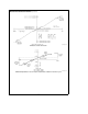
Owner's manual
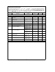
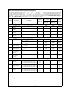
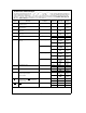


AC Electrical Characteristics
The following specifications apply for (V
a
e
V
A
a
e
V
D
a
ea
5V, V
REF
a
ea
4.096V, and fully-differential input with fixed
2.048V common-mode voltage) or (V
a
e
V
A
a
e
V
D
a
ea
3.3V, V
REF
a
ea
2.5V and fully-differential input with fixed
1.250V common-mode voltage), V
REF
b
e
0V, 12-bit
a
sign conversion mode, source impedance for analog inputs, V
REF
b
and V
REF
a
s
25X,f
CK
e
f
SK
e
5 MHz, and 10 (t
CK
) acquisition time unless otherwise specified. Boldface limits apply for
T
A
e
T
J
e
T
MIN
to T
MAX
; all other limits T
A
e
T
J
e
25
§
C. (Note 17) (Continued)
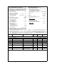
Symbol Parameter Conditions
Typical Limits Units
(Note 10) (Note 11) (Limits)
t
HPU
Hardware Power-Up Time, Time from
500 700 ms (max)
PD Falling Edge to EOC Rising Edge
t
SPU
Software Power-Up Time, Time from
Serial Data Clock Falling Edge to 500 700 ms (max)
EOC Rising Edge
t
ACC
Access Time Delay from
25 60 ns (max)
CS
Falling Edge to DO Data Valid
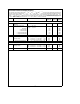
t
SET-UP
Set-Up Time of CS Falling Edge to
50 ns (min)
Serial Data Clock Rising Edge
t
DELAY
Delay from SCLK Falling
0 5 ns (min)
Edge to CS
Falling Edge
t
1H
,t
0H
Delay from CS Rising Edge to R
L
e
3k, C
L
e
100 pF
70 100 ns (max)
DO TRI-STATE
É
t
HDI
DI Hold Time from Serial Data
5 15 ns (min)
Clock Rising Edge
t
SDI
DI Set-Up Time from Serial Data
5 10 ns (min)
Clock Rising Edge
t
HDO
DO Hold Time from Serial Data R
L
e
3k, C
L
e
100 pF
35
65 ns (max)
Clock Falling Edge 5 ns (min)
t
DDO
Delay from Serial Data Clock
50 90 ns (max)
Falling Edge to DO Data Valid
t
RDO
DO Rise Time, TRI-STATE to High R
L
e
3k, C
L
e
100 pF 10 40 ns (max)
DO Rise Time, Low to High 10 40 ns (max)
t
FDO
DO Fall Time, TRI-STATE to Low R
L
e
3k, C
L
e
100 pF 15 40 ns (max)
DO Fall Time, High to Low 15 40 ns (max)
t
CD
Delay from CS Falling Edge
45 80 ns (max)
to DOR
Falling Edge
t
SD
Delay from Serial Data Clock Falling
45 80 ns (max)
Edge to DOR
Rising Edge
C
IN
Capacitance of Logic Inputs 10 pF
C
OUT
Capacitance of Logic Outputs 20 pF
8