
Owner's manual

Application Hints (Continued)
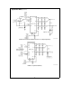
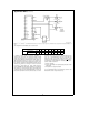
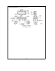
TL/H/12079–46
Note: V
A
a
,V
D
a
, and V
REF
a
on the ADC12138 each have 0.01 mF and 0.1 mF chip caps, and 10 mF tantalum caps. All logic devices are bypassed with 0.1 mF
caps.
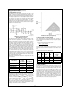
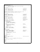
The assignment of the RS232 port is shown below
B7 B6 B5 B4 B3 B2 B1 B0
COM1
Input Address 3FE X X X CTS X X X X
Output Address 3FC X X X 0 X X RTS DTR
A sample program, written in Microsoft QuickBasic, is
shown on the next page. The program prompts for data
mode select instruction to be sent to the A/D. This can be
found from the Mode Programming table shown earlier. The
data should be entered in ‘‘1’’s and ‘‘0’’s as shown in the
table with DI0 first. Next the program prompts for the num-
ber of SCLKs required for the programmed mode select in-
struction. For instance, to send all ‘‘0’’s to the A/D, selects
CH0 as the
a
input, CH1 as the
b
input, 12-bit conversion,
and 13-bit MSB first data output format (if the sign bit was
not turned off by a previous instruction). This would require
13 SCLK periods since the output data format is 13 bits. The
part powers up with No Auto Cal, No Auto Zero, 10 CCLK
Acquisition Time, 12-bit conversion, data out with sign, pow-
er up, 12- or 13-bit MSB First, and user mode. Auto Cal,
Auto Zero, Power Up and Power Down instructions do not
change these default settings. Since there is no CS
signal to
synchronize the serial interface the following power up se-
quence should be followed:
1. Run the program
2. Prior to responding to the prompt apply the power to the
ADC12138
3. Respond to the program prompts
It is recommended that the first instruction issued to the
ADC12138 be Auto Cal (see Section 1.1).
35