
Owner's manual

Application Hints (Continued)
11.0 CLOCK SIGNAL LINE ISOLATION
The ADC12130/2/8’s performance is optimized by routing
the analog input/output and reference signal conductors as
far as possible from the conductors that carry the clock sig-
nals to the CCLK and SCLK pins. Ground traces parallel to
the clock signal traces can be used on printed circuit boards
to reduce clock signal interference on the analog input/out-
put pins.
12.0 THE CALIBRATION CYCLE
A calibration cycle needs to be started after the power sup-
plies, reference, and clock have been given enough time to
stabilize after initial turn-on. During the calibration cycle, cor-
rection values are determined for the offset voltage of the
sampled data comparator and any linearity and gain errors.
These values are stored in internal RAM and used during an
analog-to-digital conversion to bring the overall full-scale,
offset, and linearity errors down to the specified limits. Full-
scale error typically changes
g
0.4 LSB over temperature
and linearity error changes even less; therefore it should be
necessary to go through the calibration cycle only once af-
ter power up if the Power Supply Voltage and the ambient
temperature do not change significantly (see the curves in
the Typical Performance Characteristics).
13.0 THE AUTO-ZERO CYCLE
To correct for any change in the zero (offset) error of the
A/D, the auto-zero cycle can be used. It may be necessary
to do an auto-zero cycle whenever the ambient temperature
or the power supply voltage change significantly. (See the
curves titled ‘‘Zero Error Change vs Ambient Temperature’’
and ‘‘Zero Error Change vs Supply Voltage’’ in the Typical
Performance Characteristics.)
14.0 DYNAMIC PERFORMANCE
Many applications require the A/D converter to digitize AC
signals, but the standard DC integral and differential nonlin-
earity specifications will not accurately predict the A/D con-
verter’s performance with AC input signals. The important
specifications for AC applications reflect the converter’s
ability to digitize AC signals without significant spectral er-
rors and without adding noise to the digitized signal. Dynam-
ic characteristics such as signal-to-noise (S/N), signal-to-
noise
a
distortion ratio (S/(N
a
D)), effective bits, full pow-
er bandwidth, aperture time and aperture jitter are quantita-
tive measures of the A/D converter’s capability.
An A/D converter’s AC performance can be measured us-
ing Fast Fourier Transform (FFT) methods. A sinusoidal
waveform is applied to the A/D converter’s input, and the
transform is then performed on the digitized waveform.
S/(N
a
D) and S/N are calculated from the resulting FFT
data, and a spectral plot may also be obtained. Typical val-
ues for S/N are shown in the table of Electrical Characteris-
tics, and spectral plots of S/(N
a
D) are included in the
typical performance curves.
The A/D converter’s noise and distortion levels will change
with the frequency of the input signal, with more distortion
and noise occurring at higher signal frequencies. This can
be seen in the S/(N
a
D) versus frequency curves. These
curves will also give an indication of the full power band-
width (the frequency at which the S/(N
a
D) or S/N drops
3 dB).
Effective number of bits can also be useful in describing the
A/D’s noise performance. An ideal A/D converter will have
some amount of quantization noise, determined by its reso-
lution, which will yield an optimum S/N ratio given by the
following equation:
S/N
e
(6.02
c
n
a
1.8) dB
where n is the A/D’s resolution in bits.
The effective bits of a real A/D converter, therefore, can be
found by:
n(effective)
e
S/N(dB)
b
1.8
6.02
As an example, this device with a differential signed 5V,
10 kHz sine wave input signal will typically have a S/N of
78 dB, which is equivalent to 12.6 effective bits.
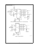
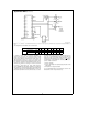
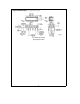
15.0 AN RS232 SERIAL INTERFACE
Shown on the following page is a schematic for an RS232
interface to any IBM and compatible PCs. The DTR, RTS,
and CTS RS232 signal lines are buffered via level transla-
tors and connected to the ADC12138’s DI, SCLK, and DO
pins, respectively. The D flip/flop is used to generate the CS
signal.
34