
Owner's manual

Application Hints (Continued)
3.0 REFERENCE VOLTAGE
The difference in the voltages applied to the V
REF
a
and
V
REF
b
defines the analog input span (the difference be-
tween the voltage applied between two multiplexer inputs or
the voltage applied to one of the multiplexer inputs and ana-
log ground), over which 4095 positive and 4096 negative
codes exist. The voltage sources driving V
REF
a
or V
REF
b
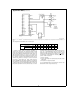
must have very low output impedance and noise. The circuit
in
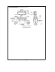
Figure 14
is an example of a very stable reference appro-
priate for use with the device.
*Tantalum
TL/H/12079–43
FIGURE 14. Low Drift Extremely
Stable Reference Circuit
The ADC12130/2/8 can be used in either ratiometric or ab-
solute reference applications. In ratiometric systems, the
analog input voltage is proportional to the voltage used for
the ADC’s reference voltage. When this voltage is the sys-
tem power supply, the V
REF
a
pin is connected to V
A
a
and
V
REF
b
is connected to ground. This technique relaxes the
system reference stability requirements because the analog
input voltage and the ADC reference voltage move togeth-
er. This maintains the same output code for given input con-
ditions. For absolute accuracy, where the analog input volt-
age varies between very specific voltage limits, a time and
temperature stable voltage source can be connected to the
reference inputs. Typically, the reference voltage’s magni-
tude will require an initial adjustment to null reference volt-
age induced full-scale errors.
Below are recommended references along with some key
specifications.
Output
Temperature
Part Number Voltage
Coefficient
Tolerance
LM4041CI-Adj
g
0.5%
g
100ppm/
§
C
LM4040AI-4.1
g
0.1%
g
100ppm/
§
C
LM9140BYZ-4.1
g
0.5%
g
25ppm/
§
C
LM368Y-5.0
g
0.1%
g
20ppm/
§
C
Circuit of
Figure 14
Adjustable
g
2ppm/
§
C
The reference voltage inputs are not fully differential. The
ADC12130/2/8 will not generate correct conversions or
comparisons if V
REF
a
is taken below V
REF
b
. Correct con-
versions result when V
REF
a
and V
REF
b
differ by 1V and
remain, at all times, between ground and V
A
a
. The V
REF
common mode range, (V
REF
a
a
V
REF
b
)/2 is restricted to
(0.1
c
V
A
a
) to (0.6
c
V
A
a
). Therefore, with V
A
a
e
5V
the center of the reference ladder should not go below 0.5V
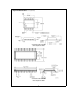
or above 3.0V.
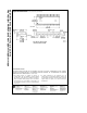
Figure 15
is a graphic representation of the
voltage restrictions on V
REF
a
and V
REF
b
.
TL/H/12079–44
FIGURE 15. V
REF
Operating Range
4.0 ANALOG INPUT VOLTAGE RANGE
The ADC12130/2/8’s fully differential ADC generate a
two’s complement output that is found by using the equation
shown below:
for (12-bit) resolution the Output Code
e
(V
IN
a
b
V
IN
b
) (4096)
(V
REF
a
b
V
REF
b
)
Round off to the nearest integer value between
b
4096 to
4095 if the result of the above equation is not a whole num-
ber.
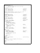
Examples are shown in the table below:
Digital
V
REF
a
V
REF
b
V
IN
a
V
IN
b
Output
Code
a
2.5V
a
1V
a
1.5V 0V 0,1111,1111,1111
a
4.096V 0V
a
3V 0V 0,1011,1011,1000
a
4.096V 0V
a
2.499V
a
2.500V 1,1111,1111,1111
a
4.096V 0V 0V
a
4.096V 1,0000,0000,0000
5.0 INPUT CURRENT
At the start of the acquisition window (t
A
) a charging current
flows into or out of the analog input pins (A/DIN1 and
A/DIN2) depending on the input voltage polarity. The ana-
log input pins are CH0 –CH7 and COM when A/DIN1 is tied
to MUXOUT1 and A/DIN2 is tied to MUXOUT2. The peak
value of this input current will depend on the actual input
voltage applied, the source impedance and the internal mul-
tiplexer switch on resistance. With MUXOUT1 tied to
A/DIN1 and MUXOUT2 tied to A/DIN2 the internal multi-
plexer switch on resistance is typically 1.6 kX. The A/DIN1
and A/DIN2 mux on resistance is typically 750X.
32