
Owner's manual


Application Hints (Continued)
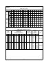
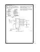
For pseudo-differential signed operation, the biasing circuit
shown in
Figure 10
shows a signal AC coupled to the ADC.
This gives a digital output range of
b
4096 to
a
4095. With a
2.5V reference, as shown, 1 LSB is equal to 610 mV. Al-
though, the ADC is not production tested with a 2.5V refer-
ence, when V
A
a
and V
D
a
are
a
5.0V linearity error typical-
ly will not change more than 0.1 LSB (see the curves in the
Typical Electrical Characteristics Section). With the ADC set
to an acquisition time of 10 clock periods, the input biasing
resistor needs to be 600X or less. Notice though that the
input coupling capacitor needs to be made fairly large to
bring down the high pass corner. Increasing the acquisition
time to 34 clock periods (with a 5 MHz CCLK frequency)
would allow the 600X to increase to 6k, which with a 1 mF
coupling capacitor would set the high pass corner at 26 Hz.
Increasing R, to 6k would allow R
2
to be 2k.
TL/H/12079–39
FIGURE 10. Pseudo-Differential Biasing with the Signal Source AC Coupled Directly into the ADC
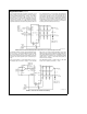
An alternative method for biasing pseudo-differential opera-
tion is to use the
a
2.5V from the LM9140 to bias any ampli-
fier circuits driving the ADC as shown in
Figure 11.
The
value of the resistor pull-up biasing the LM9140-2.5 will de-
pend upon the current required by the op amp biasing cir-
cuitry.
In the circuit of
Figure 11
some voltage range is lost since
the amplifier will not be able to swing to
a
5V and GND
with a single
a
5V supply. Using an adjustable version of the
LM4041 to set the full scale voltage at exactly 2.048V and a
lower grade LM4040D-2.5 to bias up everything to 2.5V as
shown in
Figure 12
will allow the use of all the ADC’s digital
output range of
b
4096 to
a
4095 while leaving plenty of
head room for the amplifier.
Fully differential operation is shown in
Figure 13.
One LSB
for this case is equal to (4.1V/4096)
e
1 mV.
TL/H/12079–40
FIGURE 11. Alternative Pseudo-Differential Biasing
30