
Owner's manual


Application Hints (Continued)
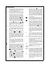
With the single-ended multiplexer configuration CH0
through CH7 can be assigned to the MUXOUT1 pin. The
COM pin is always assigned to the MUXOUT2 pin. A/DIN1
is assigned as the positve input; A/DIN2 is assigned as the
negative input. (See
Figure 8
).
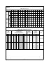
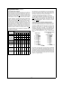
Differential
Configuration
TL/H/12079–36
A/DIN1 and A/DIN2 can be as-
signed as the
a
or
b
input
FIGURE 8
Single-Ended
Configuration
TL/H/12079–37
A/DIN1 is
a
input
A/DIN2 is
b
input
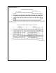
The Multiplexer assignment tables for the ADC12130/2/8
(Tables II and III) summarize the aforementioned functions
for the different versions of A/Ds.
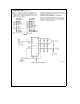
2.1 Biasing for Various Multiplexer Configurations
Figure 9
is an example of biasing the device for single-end-
ed operation. The sign bit is always low. The digital output
range is 0 0000 0000 0000 to 0 1111 1111 1111. One LSB
is equal to 1 mV (4.1V/4096 LSBs).
TL/H/12079–38
FIGURE 9. Single-Ended Biasing
29