
Owner's manual


Application Hints (Continued)
1.6 User Mode and Test Mode
An instruction may be issued to the ADC to put it into test
mode. Test mode is used by the manufacturer to verify com-
plete functionality of the device. During test mode CH0 –
CH7 become active outputs. If the device is inadvertently
put into the test mode with CS
continuously low, the serial
communications may be desynchronized. Synchronization
may be regained by cycling the power supply voltage to the
device. Cycling the power supply voltage will also set the
device into user mode. If CS
is used in the serial interface,
the ADC may be queried to see what mode it is in. This is
done by issuing a ‘‘read STATUS register’’ instruction to the
ADC. When bit 9 of the status register is high, the ADC is in
test mode; when bit 9 is low the ADC, is in user mode. As an
alternative to cycling the power supply, an instruction se-
quence may be used to return the device to user mode. This
instruction sequence must be issued to the ADC using CS
.
The following table lists the instructions required to return
the device to user mode:
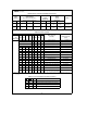
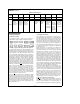
Instruction
DI Data
DI0 DI1 DI2 DI3 DI4 DI5 DI6 DI7
TEST MODE HXXXHHHH
Instructions
Test Mode
Reset
LLLLHHHL
LLLLHLHL
LLLLHLHH
USER MODE LLLLHHHH
Power Up L L L L H L H L
Set DO with H
or without or L L L H H L H
Sign L
Set H H
Acquisition or or L L H H H L
Time L L
Start H H H H H H H
a orororor L ororor
Conversion L L L L L L L
X
e
Don’t Care
After returning to user mode with the user mode instruction
the power up, data with or without sign, and acquisition time
instructions need to be resent to ensure that the ADC is in
the required state before a conversion is started.
1.7 Reading the Data Without Starting a Conversion
The data from a particular conversion may be accessed
without starting a new conversion by ensuring that the
CONV
line is taken high during the I/O sequence. See the
Read Data timing diagrams. Table V describes the opera-
tion of the CONV
pin.
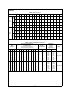
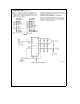
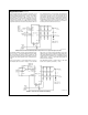
2.0 DESCRIPTION OF THE ANALOG MULTIPLEXER
For the ADC12138, the analog input multiplexer can be con-
figured with 4 differential channels or 8 single ended chan-
nels with the COM input as the zero reference or any combi-
nation thereof (see
Figure 7
). The difference between the
voltages on the V
REF
a
and V
REF
b
pins determines the
input voltage span (V
REF
). The analog input voltage range is
0toV
A
a
. Negative digital output codes result when V
IN
b
l
V
IN
a
. The actual voltage at V
IN
b
or V
IN
a
cannot go below
AGND.
4 Differential
Channels
TL/H/12079–34
FIGURE 7
CH0, CH2, CH4, and CH6 can be assigned to the MUX-
OUT1 pin in the differential configuration, while CH1, CH3,
CH5, and CH7 can be assigned to the MUXOUT2 pin. In the
differential configuration, the analog inputs are paired as fol-
lows: CH0 with CH1, CH2 with CH3, CH4 with CH5 and CH6
with CH7. The A/DIN1 and A/DIN2 pins can be assigned
positive or negative polarity.
8 Single-Ended Channels
with COM
as Zero Reference
TL/H/12079–35
28