
Owner's manual


Application Hints (Continued)
it will expect to see 13 SCLK pulses for each I/O transmis-
sion. The number of SCLK pulses that the ADC expects to
see is the same as the digital output word length. The digital
output word length is controlled by the Data Out (DO) for-
mat. The DO format maybe changed any time a conversion
is started or when the sign bit is turned on or off. The table
below details out the number of clock periods required for
different DO formats:
Number of
DO Format SCLKs
Expected
12-Bit MSB or LSB First SIGN OFF 12
SIGN ON 13
16-Bit MSB or LSB first SIGN OFF 16
SIGN ON 17
If erroneous SCLK pulses desynchronize the communica-
tions, the simplest way to recover is by cycling the power
supply to the device. Not being able to easily resynchronize
the device is a shortcoming of leaving CS
low continuously.
The number of clock pulses required for an I/O exchange
may be different for the case when CS
is left low continu-
ously vs the case when CS
is cycled. Take the I/O se-
quence detailed in
Figure 5
(Typical Power Supply Se-
quence) as an example. The table below lists the number of
SCLK pulses required for each instruction:
Instruction
CS
Low
CS
Strobed
Continuously
Auto Cal 13 SCLKs 8 SCLKs
Read Status 13 SCLKs 8 SCLKs
Read Status 13 SCLKs 8 SCLKs
12-Bit
a
Sign Conv 1 13 SCLKs 8 SCLKs
12-Bit
a
Sign Conv 2 13 SCLKs 13 SCLKs
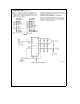
1.4 Analog Input Channel Selection
The data input on DI also selects the channel configuration
for a particular A/D conversion (see Tables II, III and IV).
In
Figure 6
the only times when the channel configuration
could be modified would be during I/O sequences 1, 4, 5
and 6. Input channels are reselected before the start of
each new conversion. Shown below is the data bit stream
required on DI, during I/O sequence number 4 in
Figure 6
,
to set CH1 as the positive input and CH0 as the negative
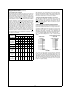
input for the different versions of ADCs:
Number
Part
DI Data
DI0 DI1 DI2 DI3 DI4 DI5 DI6 DI7
ADC12130 LHLLHLXX
and
ADC12132
ADC12138 LHLLLLHL
Where X can be a logic high (H) or low (L).
1.5 Power Up/Down
The ADC may be powered down at any time by taking the
PD pin HIGH or by the instruction input on DI (see Tables IV
and V, and the Power Up/Down timing diagrams). When the
ADC is powered down in this way, the circuitry necessary for
an A/D conversion is deactivated. The circuitry necessary
for digital I/O is kept active. Hardware power up/down is
controlled by the state of the PD pin. Software power-up/
down is controlled by the instruction issued to the ADC. If a
software power up instruction is issued to the ADC while a
hardware power down is in effect (PD pin high) the device
will remain in the power-down state. If a software power
down instruction is issued to the ADC while a hardware
power up is in effect (PD pin low), the device will power
down. When the device is powered down by software, it
may be powered up by either issuing a software power up
instruction or by taking PD pin high and then low. If the
power down command is issued during an A/D conversion,
that conversion is disrupted. Therefore, the data output after
power up cannot be relied upon.
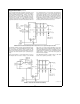
TL/H/12079–33
FIGURE 6. Changing the ADC’s Conversion Configuration
27