
Owner's manual


Pin Descriptions (Continued)
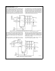
V
REF
b
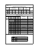
The negative voltage reference input. In order
to maintain accuracy, the voltage at this pin
must not go below GND or exceed V
A
a
. (See
Figure 4
).
V
A
a
,V
D
a
These are the analog and digital power supply
pins. V
A
a
and V
D
a
are not connected together
on the chip. These pins should be tied to the
same power supply and bypassed separately
(see
Figure 4
). The operating voltage range of
V
A
a
and V
D
a
is 3.0 V
DC
to 5.5 V
DC
.
DGND This is the digital ground pin (see
Figure 4
).
AGND This is the analog ground pin (see
Figure 4
).
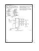
TL/H/12079–30
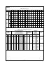
FIGURE 3. Protecting the MUXOUT1, MUXOUT2,
A/DIN1 and A/DIN2 Analog Pins
TL/H/12079–31
*Tantalum
**Monolithic Ceramic or better
FIGURE 4. Recommended Power Supply Bypassing and Grounding
23