
Owner's manual


Pin Descriptions
CCLK The clock applied to this input controls the suces-
sive approximation conversion time interval and
the acquisition time. The rise and fall times of the
clock edges should not exceed 1 ms.
SCLK This is the serial data clock input. The clock ap-
plied to this input controls the rate at which the
serial data exchange occurs. The rising edge
loads the information on the DI pin into the multi-
plexer address and mode select shift register.
This address controls which channel of the ana-
log input multiplexer (MUX) is selected and the
mode of operation for the A/D. With CS
low, the
falling edge of SCLK shifts the data resulting from
the previous ADC conversion out on DO, with the
exception of the first bit of data. When CS
is low
continuously, the first bit of the data is clocked
out on the rising edge of EOC (end of conver-
sion). When CS
is toggled, the falling edge of CS
always clocks out the first bit of data. CS should
be brought low when SCLK is low. The rise and
fall times of the clock edges should not exceed
1 ms.
DI This is the serial data input pin. The data applied
to this pin is shifted by the rising edge of SCLK
into the multiplexer address and mode select reg-
ister. Tables II through IV show the assignment of
the multiplexer address and the mode select
data.
DO The data output pin. This pin is an active push/
pull output when CS
is low. When CS is high, this
output is TRI-STATE. The A/D conversion result
(DB0– DB12) and converter status data are
clocked out by the falling edge of SCLK on this
pin. The word length and format of this result can
vary (see Table I). The word length and format
are controlled by the data shifted into the multi-
plexer address and mode select register (see Ta-
ble IV).
EOC This pin is an active push/pull output and indi-
cates the status of the ADC12130/2/8. When
low, it signals that the A/D is busy with a conver-
sion, auto-calibration, auto-zero or power down
cycle. The rising edge of EOC signals the end of
one of these cycles.
CS
This is the chip select pin. When a logic low is
applied to this pin, the rising edge of SCLK shifts
the data on DI into the address register. This low
also brings DO out of TRI-STATE. With CS
low,
the falling edge of SCLK shifts the data resulting
from the previous ADC conversion out on DO,
with the exception of the first bit of data. When
CS
is low continuously, the first bit of the data is
clocked out on the rising edge of EOC (end of
conversion). When CS
is toggled, the falling edge
of CS
always clocks out the first bit of data. CS
should be brought low when SCLK is low. The
falling edge of CS
resets a conversion in progress
and starts the sequence for a new conversion.
When CS
is brought back low during a conver-
sion, that conversion is prematurely terminated.
The data in the output latches may be corrupted.
Therefore, when CS
is brought back low during a
conversion in progress the data output at that
time should be ignored. CS
may also be left
continuously low. In this case it is imperative
that the correct number of SCLK pulses be ap-
plied to the ADC in order to remain synchro-
nous. After the ADC supply power is applied it
expects to see 13 clock pulses for each I/O
sequence. The number of clock pulses the ADC
expects is the same as the digital output word
length. This word length can be modified by the
data shifted in on the DO pin. Table IV details
the data required.
DOR
This is the data output ready pin. This pin is an
active push/pull output. It is low when the con-
version result is being shifted out and goes high
to signal that all the data has been shifted out.
CONV
A logic low is required on this pin to program
any mode or change the ADC’s configuration as
listed in the Mode Programming Table (Table
IV) such as 12-bit conversion, Auto Cal, Auto
Zero etc. When this pin is high the ADC is
placed in the read data only mode. While in the
read data only mode, bringing CS
low and puls-
ing SCLK will only clock out on DO any data
stored in the ADCs output shift register. The
data on DI will be neglected. A new conversion
will not be started and the ADC will remain in
the mode and/or configuration previously pro-
grammed. Read data only cannot be performed
while a conversion, Auto-Cal or Auto-Zero are
in progress.
PD This is the power down pin. When PD is high
the A/D is powered down; when PD is low the
A/D is powered up. The A/D takes a maximum
of 700 ms to power up after the command is
given.
CH0– CH7 These are the analog inputs of the MUX. A
channel input is selected by the address infor-
mation at the DI pin, which is loaded on the
rising edge of SCLK into the address register
(see Tables II and III).
The voltage applied to these inputs should not
exceed V
A
a
or go below GND. Exceeding this
range on an unselected channel will corrupt the
reading of a selected channel.
COM This pin is another analog input pin. It is used as
a pseudo ground when the analog multiplexer is
single-ended.
MUXOUT1, These are the multiplexer output pins.
MUXOUT2
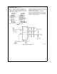
A/DIN1, These are the converter input pins. MUXOUT1
A/DIN2 is usually tied to A/DIN1. MUXOUT2 is usually
tied to A/DIN2. If external circuitry is placed be-
tween MUXOUT1 and A/DIN1, or MUXOUT2
and A/DIN2 it may be necessary to protect
these pins. The voltage at these pins should not
exceed V
A
a
or go below AGND (see
Figure 3
).
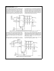
V
REF
a
This is the positive analog voltage reference in-
put. In order to maintain accuracy, the voltage
range of V
REF
(V
REF
e
V
REF
a
b
V
REF
b
)is
1V
DC
to 5.0 V
DC
and the voltage at V
REF
a
cannot exceed V
A
a
. See
Figure 4
for recom-
mended bypassing.
22