
Owner manual

Electrical Characteristics (Continued)
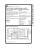
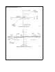
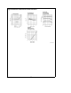
Note 9: A diode exists between AV
a
and DV
a
as shown below.
TL/H/11225–5
To guarantee accuracy, it is required that the AV
a
and DV
a
be connected together to a power supply with separate bypass filter at each V
a
pin.
Note 10: Typicals are at T
J
e
T
A
e
25
§
C and represent most likely parametric norm.
Note 11: Tested limits are guaranteed to National’s AOQL (Average Outgoing Quality Level).
Note 12: One LSB is referenced to 10 bits of resolution.
Note 13: Total unadjusted error includes offset, full-scale, linearity, multiplexer, and hold step errors.
Note 14: For DC Common Mode Error the only specification that is measured is offset error.
Note 15: Channel leakage current is measured after the channel selection.
Note 16: All the timing specifications are tested at the TTL logic levels, V
IL
e
0.8V for a falling edge and V
IH
e
2.0V for a rising.
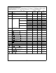
Ordering Information
Industrial
b
40
§
C
s
T
A
s
85
§
C Package
ADC10154CIN N24A
ADC10154CIWM M24B
ADC10158CIN N28B
ADC10158CIWM M28B
7