
Owner manual

Electrical Characteristics
The following specifications apply for V
a
e
AV
a
e
DV
a
ea
5.0 V
DC
,V
REF
ae
5.000 V
DC
,V
REF
be
GND, V
b
e
GND
for unipolar operation or V
b
eb
5.0 V
DC
for bipolar operation, t
r
e
t
f
e
3 ns and f
CLK
e
5.0 MHz unless otherwise specified.
Boldface limits apply for T
A
e
T
J
e
T
MIN
to T
MAX
; all other limits T
A
e
T
J
e
25
§
C. (Note 16) (Continued)
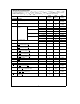
Symbol Parameter Conditions
Typical
(Note 11)
Limits
(Limit)
Units
(Note 10)
AC CHARACTERISTICS (Continued)
t
1H
,t
0H
TRI-STATE Control (Delay from C
L
e
10 pF, R
L
e
1kX
20 35 ns (Max)
Rising Edge of RD
to Hi-Z State)
t
RR
Delay between Successive
25 50 ns (Min)
RD
Pulses
t
P
Delay between Last Rising Edge
of RD
and the Next Falling 20 50 ns (Min)
Edge of WR
C
IN
Capacitance of Logic Inputs 5 pF
C
OUT
Capacitance of Logic Outputs 5 pF
Note 1: Absolute Maximum Ratings indicate limits beyond which damage to the device may occur.
Note 2: Operating Ratings indicate conditions for which the device is functional, but do not guarantee specific performance limits. For guaranteed specifications
and test conditions, see the Electrical Characteristics. The guaranteed specifications apply only for the test conditions listed. Some performance characteristics
may degrade when the device is not operated under the listed test conditions.
Note 3: All voltages are measured with respect to GND, unless otherwise specified.
Note 4: When the input voltage (V
IN
) at any pin exceeds the power supplies (V
IN
k
V
b
or V
IN
l
AV
a
or DV
a
), the current at that pin should be limited to 5 mA.
The 20 mA maximum package input current rating limits the number of pins that can safely exceed the power supplies with an input current of 5 mA to four.
Note 5: The maximum power dissipation must be derated at elevated temperatures and is dictated by T
Jmax
, i
JA
and the ambient temperature, T
A
. The maximum
allowable power dissipation at any temperature is P
D
e
(T
Jmax
b
T
A
)/i
JA
or the number given in the Absolute Maximum Ratings, whichever is lower. For this
device, T
Jmax
e
150
§
C. The typical thermal resistance (i
JA
) of these parts when board mounted follow: ADC10154 with BIN and CIN suffixes 65
§
C/W, ADC10154
with BIJ, CIJ and CMJ suffixes 49
§
C/W, ADC10154 with BIWM and CIWM suffixes 72
§
C/W, ADC10158 with BIN and CIN suffixes 59
§
C/W, ADC10158 with BIJ, CIJ,
and CMJ suffixes 46
§
C/W, ADC10158 with BIWM and CIWM suffixes 68
§
C/W.
Note 6: Human body model, 100 pF capacitor discharged through a 1.5 kX resistor.
Note 7: See AN-450 ‘‘Surface Mounting Methods and Their Effect on Product Reliability’’ or the section titled ‘‘Surface Mount’’ found in any post-1986 National
Semiconductor Linear Data Book for other methods of soldering surface mount devices.
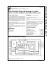
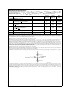
Note 8: Two on-chip diodes are tied to each analog input as shown below. They will forward-conduct for analog input voltages one diode drop below V
b
supply or
TL/H/11225–4
one diode drop greater than V
a
supply. Be careful during testing at low V
a
levels (4.5V), as high level analog inputs (5V) can cause an input diode to conduct,
especially at elevated temperatures, which will cause errors for analog inputs near full-scale. The specification allows 50 mV forward bias of either diode; this
means that as long as the analog V
IN
does not exceed the supply voltage by more than 50 mV, the output code will be correct. Exceeding this range on an
unselected channel will corrupt the reading of a selected channel. This means that if AV
a
and DV
a
are minimum (4.5 V
DC
) and V
b
is a maximum (
b
4.5 V
DC
) full
scale must be
s
g
4.55 V
DC
.
6