
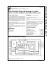
Owner manual
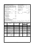

Electrical Characteristics
The following specifications apply for V
a
e
AV
a
e
DV
a
ea
5.0 V
DC
,V
REF
ae
5.000 V
DC
,V
REF
be
GND, V
b
e
GND
for unipolar operation or V
b
eb
5.0 V
DC
for bipolar operation, t
r
e
t
f
e
3 ns and f
CLK
e
5.0 MHz unless otherwise specified.
Boldface limits apply for T
A
e
T
J
e
T
MIN
to T
MAX
; all other limits T
A
e
T
J
e
25
§
C. (Note 16) (Continued)
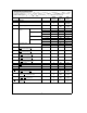
Symbol Parameter Conditions
Typical
(Note 11)
Limits
(Limit)
Units
(Note 10)
AC CHARACTERISTICS
f
CLK
Clock Frequency 8 5.0 MHz (Max)
10 kHz (Min)
Clock Duty Cycle 20 % (Min)
80 % (Max)
t
C
Conversion 8-Bit Unipolar Mode 16 1/f
CLK
Time
f
CLK
e
5.0 MHz 3.2 ms (Max)
8-Bit Bipolar Mode 18 1/f
CLK
f
CLK
e
5.0 MHz 3.6 ms (Max)
10-Bit Unipolar Mode 20 1/f
CLK
f
CLK
e
5.0 MHz 4.0 ms (Max)
10-Bit Bipolar Mode 22 1/f
CLK
f
CLK
e
5.0 MHz 4.4 ms (Max)
t
A
Acquisition Time 6 1/f
CLK
f
CLK
e
5.0 MHz 1.2 ms
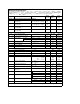
t
CR
Delay between Falling Edge of
0 5
ns (Min)
CS
and Falling Edge of RD
t
RC
Delay betwee Rising Edge
0 5 ns (Min)
RD and Rising Edge of CS
t
CW
Delay between Falling Edge
0 5 ns (Min)
of CS
and Falling Edge of WR
t
WC
Delay between Rising Edge
0 5 ns (Min)
of WR
and Rising Edge of CS
t
RW
Delay between Falling Edge
0 5 ns (Min)
of RD
and Falling Edge of WR
t
W(WR)
WR Pulse Width 25 50 ns (Min)
t
WS
WR High to CLK
d
2 Low Set-Up Time 5 ns (Max)
t
DS
Data Set-Up Time 6 15 ns (Max)
t
DH
Data Hold Time 0 5 ns (Max)
t
WR
Delay from Rising Edge
0 5 ns (Min)
of WR to Rising Edge RD
t
ACC
Access Time (Delay from Falling C
L
e
100 pF
25 45 ns (Max)
Edge of RD
to Output Data Valid)
t
WI
,t
RI
Delay from Falling Edge C
L
e
100 pF
25 40 ns (Max)
of WR
or RD to Reset of INT
t
INTL
Delay from Falling Edge of CLK
d
2 to Falling
40 ns
Edge of INT
5