
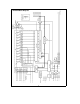
Owner manual

3.0 Applications Information (Continued)
3.2 REFERENCE CONSIDERATIONS
The voltage difference between the V
REF
a
and V
REF
b
in-
puts defines the analog input voltage span (the difference
between V
IN
(Max) and V
IN
(Min)) over which the 2
n
(where n
is the programmed resolution) possible output codes apply.
In the pseudo-differential and differential modes the actual
voltage applied to V
REF
a
and V
REF
b
can lie anywhere be-
tween the AV
a
and V
b
. Only the difference voltage is of
importance. When using the single-ended multiplexer mode
the voltage at V
REF
b
has a dual function. It simultaneously
determines the ‘‘zero’’ reference voltage and, with V
REF
a
,
the analog voltage span.
The value of the voltage on the V
REF
a
or V
REF
b
inputs
can be anywhere between AV
a
a
50 mV and V
b
b
50 mV, so long as V
REF
a
is greater than V
REF
b
. The
ADC10154 and ADC10158 can be used in either ratiometric
applications or in systems requiring absolute accuracy. The
reference pins must be connected to a voltage source capa-
ble of driving the minimum reference input resistance of
4.5 kX.
The internal 2.5V bandgap reference in the ADC10154 and
ADC10158 is available as an output on the V
REF
Out pin. To
ensure optimum performance this output needs to be by-
passed to ground with 330 mF aluminum electrolytic or tan-
talum capacitor. The reference output is unstable with ca-
pacitive loads greater than 100 pF and less than 100 mF.
Any capacitive loads
s
100 pF or
t
100 mF will not cause
the reference to oscillate. Lower output noise can be ob-
tained by increasing the output capacitance. The 330 mF
capacitor will yield a typical noise floor of 200 nVrms/
0
Hz.
The 2.5V reference output is referred to the negative supply
pin (V
b
). Therefore, the voltage at V
REF
Out will always
be 2.5V greater than the voltage applied to V
b
. Applying
this voltage to V
REF
a
with V
REF
b
tied to V
b
will yield an
analog voltage span of 2.5V. In bipolar operation the volt-
age at V
REF
Out will be at
b
2.5V when V
b
is tied to
b
5V.
For the single-ended multiplexer mode the analog input volt-
age range will be from
b
5V to
b
2.5V. The pseudo-differen-
tial and differential multiplexer modes allow for more flexibil-
ity in the analog input voltage range since the ‘‘zero’’ refer-
ence voltage is set by the actual voltage applied to the as-
signed negative input pin. The drawback of using the inter-
nal reference in the bipolar mode is that any noise on the
b
5V tied to the V
b
pin will affect the conversion result. The
bandgap reference is specified and tested in unipolar opera-
tion with V
b
tied to the system ground.
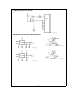
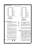
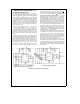
In a ratiometric system
(Figure 4a)
, the analog input voltage
is proportional to the voltage used for the A/D reference.
This voltage may also be the system power supply, so
V
REF
a
can also be tied to AV
a
. This technique relaxes the
stablity requirements of the system reference as the analog
input and A/D reference move together maintaining the
same output code for a given input condition.
For absolute accuracy
(Figure 4b)
, where the analog input
varies between very specific voltage limits, the reference pin
can be biased with a time- and temperature-stable voltage
source that has excellent initial accuracy. The LM4040 and
LM185 references are suitable for use with the ADC10154
and ADC10158.
TL/H/11225–21
a. Ratiometric Using the Internal Reference
TL/H/11225–22
b. Absolute Using a 4.096V Span
FIGURE 4. Different Reference Configurations
19