
Owner manual

2.0 Functional Description
The ADC10154 and ADC10158 use successive approxima-
tion to digitize an analog input voltage. Additional logic has
been incorporated in the devices to allow for the programm-
ability of the resolution, conversion time and digital output
format. A capacitive array and a resistive ladder structure
are used in the DAC portion of the A/D converters. The
structure of the DAC allows a very simple switching scheme
to provide a very versatile analog input multiplexer. Also,
inherent in this structure is a sample/hold. A 2.5V CMOS
band-gap reference is also provided on the ADC10154 and
ADC10158.
2.1 DIGITAL INTERFACE
The ADC10154 and ADC10158 have eight digital outputs
(DB0–DB8) and can be easily interfaced to an 8-bit data
bus. Taking CS
and WR low simultaneously will strobe the
data word on the data-bus into the input latch. This word will
be decoded to determine the multiplexer channel selection,
the A/D conversion resolution and the output data format.
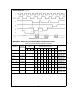
The following table shows the input word data-bit assign-
ment.
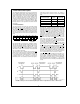
DB0 DB1 DB2 DB3 DB4 DB5 DB6 DB7
MA0 MA1 MA2 MA3 MA4 U/S 8/10 L/R
X ä YX ä Y
MUX Address Control
Input Data
DB0 through DB4 are assigned to the multiplexer address
data bits zero through four (MA0–MA4). Tables II and III
describe the multiplexer address assignment. DB5 selects
unsigned or signed (U/S
) operation. DB6 selects 8- or 10-bit
resolution. DB7 selects left or right justification of the output
data. Refer to Table I for the effect the Control Input Data
has on the digital output word.
The conversion process is started by the rising edge of WR
,
which sets the ‘‘start conversion’’ bit inside the ADC. If this
bit is set, the converter will start acquiring the input voltage
on the next falling edge of the internal CLK
d
2 signal. The
acquisition period is 3 CLK
d
2 periods, or 6 CLK periods.
Immediately after the acquisition period the input signal is
held and the actual conversion begins. The number of
clocks required for a conversion is given in the following
table:
Conversion Type
CLK
d
2 CLK
Cycles Cycles (N)
8-Bit 8 16
8-Bit
a
Sign 9 18
10-Bit 10 20
10-Bit
a
Sign 11 22
Since the CLK
d
2 signal is internal to the ADC, it is initially
impossible to know which falling edge of CLK corresponds
to the falling edge of CLK
d
2. For the first conversion, the
rising edge of WR
should occur at least t
WS
ns before any
falling edge of CLK. If this edge happens to be on the rising
edge of CLK
d
2, this will add 2 CLK cycles to the total con-
version time. The phase of the CLK
d
2 signal can be deter-
mined at the end of the first conversion, when INT
goes low.
INT
always goes low on the falling edge of the CLK
d
2 sig-
nal. From the first falling edge of INT
onward, every other
falling edge of CLK will correspond to the falling edge of
CLK
d
2. With the phase of CLK
d
2 now known, the conver-
sion time can be minimized by taking WR
high at least t
WS
ns before the falling edge of CLK
d
2.
Upon completion of the conversion, INT goes low to signal
the A/D conversion result is ready to be read. Taking CS
and RD low will enable the digital output buffer and put byte
1 of the conversion result on DB0 through DB7. The falling
edge of RD
resets the INT output high. Taking CS and RD
low a second time will put byte 2 of the conversion result on
DB7–DB0. Table I defines the DB0– DB7 assignement for
different Control Input Data. The second read does not have
to be completed before a new conversion is started.
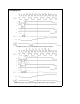
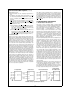
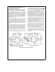
Taking CS
,WRand RD low simultaneously will start a con-
version without changing the multiplexer channel assign-
ment or output configuration and resolution. The timing dia-
gram in
Figure 2
shows the sequence of events that imple-
ment this function. Refer to Diagrams 1, 2, and 3 in the
Timing Diagrams section for the timing constraints that must
be met.
TL/H/11225–19
FIGURE 2. Starting a Conversion without Updating the Channel Configuration, Resolution, or Data Format
17