
Owner manual
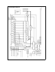

Connection Diagrams
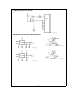
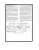
Dual-In Line and SO Packages
TL/H/11225–2
Top View
Order Number ADC10154
NS Package Numbers
J24A, M24B or N24A
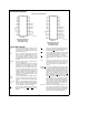
TL/H/11225–3
Top View
Order Number ADC10158
NS Package Numbers
J28A, M28B or N28B
1.0 Pin Descriptions
AV
a
This is the positive analog supply. This pin
should be bypassed with a 0.1 mF ceramic ca-
pacitor and a 10 mF tantalum capacitor to the
system analog ground.
DV
a
This is the positive digital supply. This supply
pin also needs to be bypassed with 0.1 mF ce-
ramic and 10 mF tantalum capacitors to the
system digital ground. AV
a
and DV
a
should
be bypassed separately and tied to same pow-
er supply.
DGND This is the digital ground. All logic levels are
referred to this ground.
V
b
This is the negative analog supply. For unipolar
operation this pin may be tied to the system
analog ground or to a negative supply source.
It should not go above DGND by more than
50 mV. When bipolar operation is required, the
voltage on this pin will limit the analog input’s
negative voltage level. In bipolar operation this
supply pin needs to be bypassed with 0.1 mF
ceramic and 10 mF tantalum capacitors to the
system analog ground.
V
REF
a
, These are the positive and negative reference
V
REF
b
inputs. The voltage difference between V
REF
a
and V
REF
b
will set the analog input voltage
span.
V
REF
Out This is the internal band-gap voltage reference
output. For proper operation of the voltage ref-
erence, this pin needs to be bypassed with a
330 mF tantalum or electrolytic capacitor.
CS
This is the chip select input. When a logic low is
applied to this pin the WR
and RD pins are
enabled.
RD
This is the read control input. When a logic low
is applied to this pin the digital outputs are en-
abled and the INT
output is reset high.
WR This is the write control input. The rising edge
of the signal applied to this pin selects the mul-
tiplexer channel and initiates a conversion.
INT
This is the interrupt output. A logic low at this
output indicates the completion of a conver-
sion.
CLK This is the clock input. The clock frequency di-
rectly controls the duration of the conversion
time (for example, in the 10-bit bipolar mode
t
C
e
22/f
CLK
) and the acquisition time (t
A
e
6/f
CLK
).
DB0(MA0)– These are the digital data inputs/outputs. DB0
DB7 (L/R
) is the least significant bit of the digital output
word; DB7 is the most significant bit in the digi-
tal output word (see the Output Data Configura-
tion table). MA0 through MA4 are the digital
inputs for the multiplexer channel selection
(see the Multiplexer Addressing tables). U/S
(Unsigned/Signed), 8/10, (8/10-bit resolution)
and L/R
(Left/Right justification) are the digital
input bits that set the A/D’s output word format
and resolution (see the Output Data Configura-
tion table). The conversion time is modified by
the chosen resolution (see Electrical AC Char-
acteristics table). The lower the resolution, the
faster the conversion will be.
CH0–CH7 These are the analog input multiplexer chan-
nels. They can be configured as single-ended
inputs, differential input pairs, or pseudo-differ-
ential inputs (see the Multiplexer Addressing
tables for the input polarity assignments).
16