
Owner manual
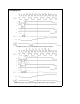
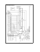
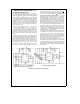

Timing Diagrams (Continued)
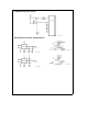
TL/H/11225–17
DIAGRAM 3. Reading the Conversion Result
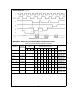
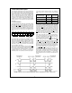
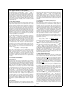
Multiplexer Addressing and Output Data Configuration Tables
TABLE I. ADC10154 and ADC10158 Output Data Configuration
Data Format
Output
Control Input
Data Bus Output Assignment
Resolution Data
8/10 U/S L/R DB7 DB6 DB5 DB4 DB3 DB2 DB1 DB0
10-Bits
a
Sign Right-Justified L L L Sign Sign Sign Sign Sign Sign MSB 9 First Byte Read
8 7 6 5 4 3 2 LSB Second Byte Read
10-Bits
a
Sign Left-Justified L L H Sign MSB 9 8 7 6 5 4 First Byte Read
3 2 LSB L L L L L Second Byte Read
10-Bits Right-Justified L H L L L L L L L MSB 9 First Byte Read
8 7 6 5 4 3 2 LSB Second Byte Read
10-Bits Left-Justified L H H MSB 9 8 7 6 5 4 3 First Byte Read
2 LSB L L L L L L Second Byte Read
8-Bits
a
Sign Right-Justified H L L Sign Sign Sign Sign Sign Sign Sign Sign First Byte Read
MSB 7 6 5 4 3 2 LSB Second Byte Read
8-Bits
a
Sign Left-Justified H L H Sign MSB 7 6 5 4 3 2 First Byte Read
LSB L L L L L L L Second Byte Read
8-Bits Right-Justified H H L L L L L L L L L First Byte Read
MSB 7 6 5 4 3 2 LSB Second Byte Read
8-Bits Left-Justified H H H MSB 7 6 5 4 3 2 LSB First Byte Read
L L L L L L L L Second Byte Read
13