
Manual

Absolute Maximum Ratings (Notes 1,
2)
If Military/Aerospace specified devices are required,
please contact the National Semiconductor Sales Office/
Distributors for availability and specifications.
Supply Voltage (V
CC
) (Note 3) 6.5V
Voltage at Any Pin −0.3V to (V
CC
+0.3V)
Except Control Inputs
Voltage at Control Inputs −0.3V to 15V
(START, OE, CLOCK, ALE, EXPANSION CONTROL,
ADD A, ADD B, ADD C, ADD D)
Storage Temperature Range −65˚C to + 150˚C
Package Dissipation at T
A
=
25˚C 875 mW
Lead Temp. (Soldering, 10 seconds)
Dual-In-Line Package (Plastic) 260˚C
Dual-In-Line Package (Ceramic) 300˚C
Molded Chip Carrier Package
Vapor Phase (60 seconds) 215˚C
Infrared (15 seconds) 220˚C
ESD Susceptibility (Note 9) 400V
Operating Conditions (Notes 1, 2)
Temperature Range (Note 1) T
MIN
≤T
A
≤T
MAX
ADC0816CCJ, ADC0816CCN, −40˚C≤T
A
≤+85˚C
ADC0817CCN
Range of V
CC
(Note 1) 4.5 V
DC
to 6.0 V
DC
Voltage at Any Pin 0V to V
CC
Except Control Inputs
Voltage at Control Inputs 0V to 15V
(START, OE, CLOCK, ALE, EXPANSION CONTROL,
ADD A, ADD B, ADD C, ADD D)
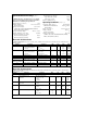
Electrical Characteristics
Converter Specifications: V
CC
=
5V
DC
=
V
REF(+)
,V
REF(−)
=
GND, V
IN
=
V
COMPARATOR IN,
T
MIN
≤T
MAX
and f
CLK
=
640 kHz unless
otherwise stated.
Symbol Parameter Conditions Min Typ Max Units
ADC0816
Total Unadjusted Error 25˚C
±
1
⁄
2
LSB
(Note 5) T
MIN
to T
MAX
±
3
⁄
4
LSB
ADC0817
Total Unadjusted Error 0˚C to 70˚C
±
1 LSB
(Note 5) T
MIN
to T
MAX
±
1
1
⁄
4
LSB
Input Resistance From Ref(+) to Ref(−) 1.0 4.5 kΩ
Analog Input Voltage Range (Note 4) V(+) or V(−) GND−0.10 V
CC
+0.10 V
DC
V
REF(+)
Voltage, Top of Ladder Measured at Ref(+) V
CC
V
CC
+0.1 V
Voltage, Center of Ladder V
CC
/2−0.1 V
CC
/2 V
CC
/2+0.1 V
V
REF(−)
Voltage, Bottom of Ladder Measured at Ref(−) −0.1 0 V
Comparator Input Current f
c
=
640 kHz, (Note 6) −2
±
0.5 2 µA
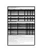
Electrical Characteristics
Digital Levels and DC Specifications: ADC0816CCJ, ADC0816CCN, ADC0817CCN — 4.75V≤V
CC
≤5.25V, −40˚C≤T
A
≤+85˚C
unless otherwise noted.
Symbol Parameter Conditions Min Typ Max Units
ANALOG MULTIPLEXER
R
ON
Analog Multiplexer ON (Any Selected Channel)
Resistance T
A
=
25˚C, R
L
=
10k 1.5 3 kΩ
T
A
=
85˚C 6 kΩ
T
A
=
125˚C 9 kΩ
∆R
ON
∆ON Resistance Between Any (Any Selected Channel) 75 Ω
2 Channels R
L
=
10k
I
OFF+
OFF Channel Leakage Current V
CC
=
5V, V
IN
=
5V,
T
A
=
25˚C 10 200 nA
T
MIN
to T
MAX
1.0 µA
I
OFF(−)
OFF Channel Leakage Current V
CC
=
5V, V
IN
=
0,
T
A
=
25˚C −200 nA
T
MIN
to T
Max
−1.0 µA
3 www.national.com