
Owner manual


6
T7024
4533A–BLURF–09/02
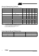
Control Logic for LNA and T/R Switch Driver
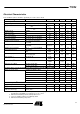
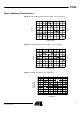
Standby current Standby, Pin VS_LNA I
S_standby
110µA
Frequency range RX f 2.4 2.5 GHz
Power gain RX, Pin LNA_IN to LNA_OUT Gp 15 16 19 dB
Noise figure RX, PSSO20
N20
NF
NF
2.5
2.1
2.8
2.3
dB
Gain compression RX,
referred to Pin LNA_OUT
O1dB -9 -7 -6 dBm
3
rd
-order input interception point RX IIP3 -16 -14 -13 dBm
Input matching
(4)
RX, Pin LNA_IN VSWRin 2:1
Output matching
(4)
RX Pin LNA_OUT VSWRout 2:1
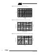
Logic input levels (RX_ON, PU)
High input level = ‘1’ Pins RX_ON and PU V
iH
2.4 V
S, LNA
V
Low input level = ‘0’ V
iL
00.5V
High input current = ‘1’ V
iH
= 2.4 V I
iH
40 60 µA
Low input current = ‘0’ I
iL
0.2 µA
Electrical Characteristics (Continued)
Test conditions (unless otherwise specified): V
S
= 3.0 V, T
amb
= 25°C
Parameters Test Conditions
Symbol Min. Typ. Max. Unit
Notes: 1. Power amplifier shall be unconditionally stable, maximum duty cycle 100%, true CW operation, maximum load mismatch
and duration: load VSWR = 10:1 (all phases) 10 s, Z
C
= 50 W.
2. With external matching network, load impedance 50
W.
3. Low-noise amplifier shall be unconditionally stable.
4. With external matching components.
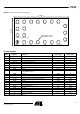
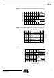
Operation Mode PU RX_ON
Standby 0 0
TX 1 0
RX 1 1