
Owner manual


5
T7024
4533A–BLURF–09/02
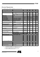
Electrical Characteristics
Test conditions (unless otherwise specified): V
S
= 3.0 V, T
amb
= 25°C
Parameters Test Conditions
Symbol Min. Typ. Max. Unit
Power Amplifier
(1)
Supply voltage Pins V1_PA, V2_PA, V3_PA_OUT V
S
2.7 3.0 4.6 V
Supply current TX PSSO20
N20
I
S_TX
I
S_TX
190
165
mA
mA
RX (PA off), V
RAMP
£ 0.1 V I
S_RX
10 µA
Standby current Standby I
S_standby
10 µA
Frequency range TX f 2.4 2.5 GHz
Gain-control range TX
DGp 60 42 dB
Power gain maximum TX, Pin PA_IN to V3_PA_OUT Gp 28 30 33 dB
Power gain minimum TX, Pin PA_IN to V3_PA_OUT Gp -40 -17 dB
Ramping voltage maximum TX, power gain (maximum)
Pin RAMP
V
RAMP max
1.7 1.75 1.83 V
Ramping voltage minimum TX, power gain (minimum)
Pin RAMP
V
RAMP min
0.1 V
Ramping current maximum TX, V
RAMP
= 1.75 V, Pin RAMP I
RAMP max
0.5 mA
Power-added efficiency TX PSSO20
N20
PAE
PAE
30
35
35
40
%
%
Saturated output power TX, input power = 0 dBm referred to
Pins V3_PA_OUT
P
sat
22.0 23 24.0 dBm
Input matching
(2)
TX, Pin PA_IN Load
VSWR
<1.5:1
Output matching
(2)
TX, Pins V3_PA_OUT Load
VSWR
<1.5:1
Harmonics at P 1dBCP TX, Pins V3_PA_OUT 2 fo -30 dBc
TX, Pins V3_PA_OUT 3 fo -30 dBc
T/R Switch Driver (Current Programming by External Resistor from R_SWITCH to GND)
Switch-out current output Standby, Pin SWITCH_OUT I
S_O_standby
1µA
RX I
S_O_RX
1µA
TX at 100
W I
S_O_100
1.7 mA
TX at 1.2 k
W I
S_O_1k2
7mA
TX at 33 k
W I
S_O_33k
17 mA
TX at
¥ I
S_O_R
19 mA
Low-noise Amplifier
(3)
Supply voltage All, Pin VS_LNA V
S
2.7 3.0 5.5 V
Supply current RX I
S
89mA
Supply current
(LNA and control logic)
TX (control logic active)
Pin VS_LNA
I
S
0.5 mA
Notes: 1. Power amplifier shall be unconditionally stable, maximum duty cycle 100%, true CW operation, maximum load mismatch
and duration: load VSWR = 10:1 (all phases) 10 s, Z
C
= 50 W.
2. With external matching network, load impedance 50
W.
3. Low-noise amplifier shall be unconditionally stable.
4. With external matching components.