
Owner manual
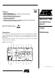


4
T7024
4533A–BLURF–09/02
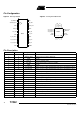
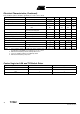
Absolute Maximum Ratings
Parameters Symbol Value Unit
Supply voltage
Pins VS_LNA, V1_PA, V2_PA, V3_PA_OUT
V
S
6V
Junction temperature T
j
150 °C
Storage temperature T
stg
-40 to +125 °C
RF input power LNA P
inLNA
5dBm
RF input power PA P
inPA
10 dBm
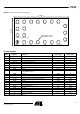
Thermal Resistance
Parameters Symbol Value Unit
Junction ambient PSSOP20, slug soldered on PCB R
thJA
19 K/W
Junction ambient HP-VFQFP-N20, slug soldered on PCB R
thJA
27 K/W
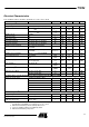
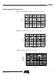
Operating Range
All voltages are referred to ground (Pins GND and slug). Power supply points are VS_LNA, V1_PA, V2_PA, V3_PA_OUT.
The table represents the sum of all supply currents depending on the TX/RX mode.
Parameters Symbol Min. Typ. Max. Unit
Supply voltage Pins V1_PA, V2_PA and
V3_PA_OUT
V
S
2.7 3.0 4.6 V
Supply voltage Pin VS_LNA V
S
2.7 3.0 5.5 V
Supply current TX PSSO20
N20
RX
I
S
I
S
I
S
190
165
8
mA
mA
mA
Standby current PU = 0 I
S_standby
10 µA
Ambient temperature T
amb
-25 +25 +70 °C