
Owner manual


2
T7024
4533A–BLURF–09/02
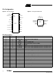
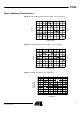
Pin Configuration
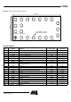
Figure 2. Pinning PSSO20 Figure 3. Pinning HP-VFQFP-N20
1
2
3
4
5
6
7
8
10
9
19
18
17
16
14
15
13
12
11
20
LNA_IN
VS_LNA
GND
V3_PA_OUT
V3_PA_OUT
V3_PA_OUT
SWITCH_OUT
GND
GND
PA_IN
V1_PA
GND
V2_PA
V2_PA
RX_ON
LNA_OUT
GND
RAMP
R_SWITCH PU
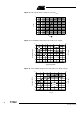
T7024
1
2
3
4
5
15
14
13
12
11
10 6789
16 2019
18
17
LNA_OUT
RX_ON
PU
R_SWITCH
SWITCH_OUT
G
N
D
V
S
_
L
N
A
G
N
D
L
N
A
_
I
N
G
N
D
V3_PA_OUT
V3_PA_OUT
V3_PA_OUT
GND
RAMP
V
2
_
P
A
V
2
_
P
A
G
N
D
V
1
_
P
A
P
A
_
I
N
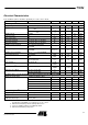
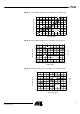
T7024
Pin Description
Pins PSSO20 Pins N20 Symbol Function
1 4 R_SWITCH Resistor to GND sets the PIN diode current
2 5 SWITCH_OUT Switched current output for PIN diode
36GNDGround
4 7 LNA_IN Low-noise amplifier input
5 9 VS_LNA Supply voltage input for low-noise amplifier
68GNDGround
7 11 V3_PA_OUT Inductor to power supply and matching network for power amplifier output
8 12 V3_PA_OUT Inductor to power supply and matching network for power amplifier output
9 13 V3_PA_OUT Inductor to power supply and matching network for power amplifier output
10 10 GND Ground
11 15 RAMP Power ramping control input
12 16 V2_PA Inductor to power supply for power amplifier
13 17 V2_PA Inductor to power supply for power amplifier
14 14 GND Ground
15 19 V1_PA Supply voltage for power amplifier
16 20 PA_IN Power amplifier input
17 18 gnd Ground
18 1 LNA_OUT Low-noise amplifier output
19 2 RX_ON RX active high
20 3 PU Power-up active high
Slug Slug GND Ground