
User guide

4
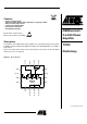
T7023
4532A–BLURF–09/02
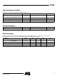
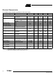
Electrical Characteristics
Test conditions (unless otherwise specified): V
S
= 3.0 V, T
amb
= 25°C
Parameters Test Conditions Symbol Min. Typ. Max. Unit
Power Amplifier
(1)
Supply voltage Pins V1_PA, V2_PA and
V3_PA_OUT
V
S
2.7 3.0 4.6 V
Supply current TX I
S_TX
165 mA
RX (PA off), V
RAMP
³ 0.1 V I
S_RX
10 µA
Standby I
S_standby
10 µA
Frequency range TX f 2.4 2.5 GHz
Gain-control range TX DGp 60 42 dB
Power gain maximum TX
Pin PA_IN to V3_PA_OUT
Gp 28 30 33 dB
Power gain minimum TX
Pin PA_IN to V3_PA_OUT
Gp -40 -17 dB
Ramping voltage maximum TX, power gain (maximum)
Pin RAMP
V
RAMP max
1.7 1.75 1.83 V
Ramping voltage minimum TX, power gain (minimum)
Pin RAMP
V
RAMP min
0.1 V
Ramping current maximum V = 1.75 V 0.5 mA
Power-added efficiency TX PAE 35 42 %
Saturated output power TX, input power = 0 dBm
referred to Pins V3_PA_OUT
P
sat
22.5 23 23.5 dBm
Input matching
(2)
TX, Pin PA_IN Load VSWR <1.5:1
Output matching
(2)
TX, Pin V3_PA_OUT Load VSWR <1.5:1
Harmonics
at P
sat
= 23 dBm
TX, Pin V3_PA_OUT
2 f
o
-30 dBc
Harmonics
at P
sat
= 23 dBm
TX, Pin V3_PA_OUT
3 f
o
-30 dBc
Notes: 1. Power amplifier shall be unconditionally stable, maximum duty cycle 100%, true CW operation, maximum load mismatch
and duration: VSWR 10:1 (all phases) 10 s, Z
G
= 50 W.
2. With external matching network, load impedance 50 W