
User guide

2
T7023
4532A–BLURF–09/02
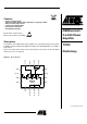
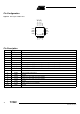
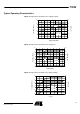
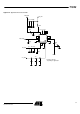
Pin Configuration
Figure 2. Pinning HP-VFQFP-N16
GND
GND
Ramp
GND
GND
GND
PA_IN
GND
V
3
_
P
A
_
O
U
T
V
3
_
P
A
_
O
U
T
V
3
_
P
A
_
O
U
T
G
N
D
V
2
_
P
A
V
2
_
P
A
G
N
D
V
1
_
P
A
8 7 6 5
13 14 15 16
9
10
11
12
4
3
2
1
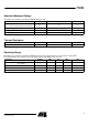
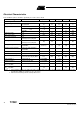
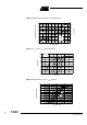
Pin Description
Pin Symbol Function
1 GND Ground
2 PA_IN Power amplifier input
3 GND Ground
4 GND Ground
5 GND Ground
6 V3_PA_OUT Inductor to power supply and matching network for power amplifier output
7 V3_PA_OUT Inductor to power supply and matching network for power amplifier output
8 V3_PA_OUT Inductor to power supply and matching network for power amplifier output
9 GND Ground
10 GND Ground
11 RAMP Power ramping control input
12 GND Ground
13 V2_PA Inductor to power supply for power amplifier
14 V2_PA Inductor to power supply for power amplifier
15 GND Ground
16 V1_PA Supply voltage for power amplifier
Slug GND Ground