
User Manual

RAE Systems by Honeywell
Honeywell Confidential and Proprietary Revision –1.0 Page 9 of 16
Copyright ©
2016
Honeywell Analytics, All rights reserved.
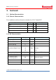
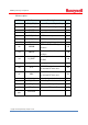
PIN description:
PIN
Pin Name
Description
I/O
4 GPIO_LED_R General Purpose Digital Output O
6 GPIO_LED_G General Purpose Digital Output O
8 RESET Reset Input (active low)
9,22,23 DGND Digital Ground
13 UART_RXD UART receive input I
14 UART_TXD UART transmit output O
24,25 D_VCC Digital Supply Voltage (Vcc)
26 SWDIO
JTAG Serial Wire Debug
Interface
I/O
29 SWCLK
JTAG Serial Wire Debug
Interface
I/O
34 A_VREF
Input/Output reference voltage
for ADC
I/O
35 A_GND Analog ground
40 CTX
RF RX/TX Indication to control
an external RF front-end
O
41 CRX
RF RX/TX Indication to control
an external RF front-end
O
43 WakeUp Wake Up Input(active low) I
44,46,48 RF_GND RF Analog Ground
45 RFP_IO Differential RF Input/Output I/O
47 RFN_IO Differential RF Input/Output I/O
Others
pins
Reserved