
User's Manual
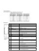


19 NC Dedicated for use with carrier board emulator/debug
module
Pin ATmega 128/64 Pin Name Description
20 PC6 Dedicated connection to green LED (DS3 on carrier
board) for debugging purposes
21 PB3 Master In/Slave Out SPI (used to configure the
EM2420)
22 PG2 General purpose I/O
23 PB2 (MOSI) Master Out/Slave In SPI (used to configure the
RM2420)
24 AVCC Analog voltage reference pin
25 PB1 (SCK) SPI clock (used to configure the RM2420)
26 AGND Analog ground pin (same as digital GND)
27 PC1 Dedicated signal for Temperature Enable (active high)
for temperature sensor on carrier board
28 AREF ADC voltage reference pin
29 NC
30 PF1 (ADC1) EmberNet stack uses alternate function ACD1 to
monitor external battery pack voltage
31 NC
32 PF2 (ADC2) EmberNet stack uses alternate function ACD2 for
temperature calibration
33 PE3 (OC3A/AIN1) General purpose I/O
34 PF4 (ADC4/TCK) General purpose I/O; if JTAG is enabled, the
EmberNet stack uses alternate function TCK for JTAG
35 PE2 (XCK0/AIN0) General Purpose I/O
36 PF5 (ADC5/TMS) General purpose I/O; if JTAG is enabled, the
EmberNet stack uses alternate function TMS for
JTAG
37 PE1 (TXD0/PDO) EmberNet stack defaults to alternate function TX
UART (TXD0)
38 PF6 (ADC6/TDO) General purpose I/O; if JTAG is enabled, the
EmberNet stack uses alternate function TDO for
JTAG
39 PE0 (RXD0/PDI) EmberNet stack defaults to alternate function RX
UART (RXD0)
40 PF7 (ADC7/TDI) General purpose I/O; if JTAG is enabled, the
EmberNet stack uses alternate function TDI for JTAG
Instructions
All users of this device must state on the outside of the host “Contains FCC ID: SU3RM2420”.
Warning (Part 15.21)
Changes or modifications not expressly approved by the party responsible for compliance could void the user’s
authority to operate the equipment.