
Installation guide
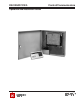


D9412G/D7412G Operation & Installation Guide
© 2002 Radionics Page 7 43488D
D9412G/D7412G
Contents
Figures:
Figure 1: System Configuration ...................................................................................................................................................13
Figure 2: Enclosure Mounting ......................................................................................................................................................21
Figure 3: Ground Fault Detect ......................................................................................................................................................22
Figure 4: Reset Pin ........................................................................................................................................................................22
Figure 5: Non Power Limited Wiring...........................................................................................................................................26
Figure 6: Charging and Battery LEDs ..........................................................................................................................................28
Figure 7: Relays for Terminals 7 and 8 and Ground Start .........................................................................................................31
Figure 8: RJ31X Wiring .................................................................................................................................................................32
Figure 9: Phone Connector and LED and Operation Monitor LED Locations ..........................................................................33
Figure 10: Phone Monitor Select .................................................................................................................................................34
Figure 11: D928 Dual Phone Line Switcher ................................................................................................................................36
Figure 12: On-board Point Sensor Loop Wiring .........................................................................................................................37
Figure 13: Wiring for Installations using the Ademco AB-12 Bell/Housing .............................................................................38
Figure 14a: Connecting the D8125 POPEX to the D9412G Panel .............................................................................................40
Figure 14b: Connecting the D8125 POPEX to the D7412G Panel .............................................................................................41
Figure 15: Program Record Sheet...............................................................................................................................................44
Figure 16a: Connecting D8128D OctoPOPITs to the D9412G ...................................................................................................47
Figure 16b: Connecting D8128D OctoPOPITs to the D7412G ...................................................................................................48
Figure 17b: D8129 Connections to the D7412G .........................................................................................................................50
Figure 17a: D8129 Connections to the D9412G .........................................................................................................................50
Figure 18a: D811 Module Wiring to the D9412G .........................................................................................................................51
Figure 18b: D811 Module Wiring to the D7412G .........................................................................................................................52
Figure 19: Power at Command Centers .....................................................................................................................................54
Figure 20: Keyswitch Wiring ........................................................................................................................................................55
Figure 21: Reset Pin ......................................................................................................................................................................61
Figure 22: Programmer and Accessory Connections ..............................................................................................................61
Figure 23a: D9412G Faceplate .....................................................................................................................................................63
Figure 23b: D7412G Faceplate .....................................................................................................................................................64
Figure 24a: D9412G System Wiring Diagram, 1 of 3 .................................................................................................................65
Figure 24b: D9412G System Wiring Diagram, 2 of 3 .................................................................................................................66
Figure 24c: D9412G System Wiring Diagram, 3 of 3 .................................................................................................................67
Figure 25a: D7412G System Wiring Diagram, 1 of 3 .................................................................................................................68
Figure 25b: D7412G System Wiring Diagram, 2 of 3 .................................................................................................................69
Figure 25c: D7412G System Wiring Diagram, 3 of 3 .................................................................................................................70