
User's Manual
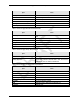
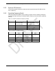
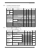
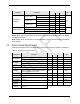
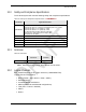
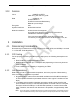
Table Of Contents
- 1 Introduction
- 2 System Description
- 3 Specifications
- 4 Installation
- 5 Scheduled and Unscheduled Maintenance
- 6 System Configuration Changes

S-Series OmniCell@Home Picocell GSM Implementation Guide Specifications
998-1027-01 Rev X2
3.8.3 Transmitter Performance Summary
Table 12 Transmitter Performance Summary
Parameter Condition
V
alue
Unit
Min Typ Max
Tx
Output
Power
Level
GMSK
GSM850, GSM900 Power Step 0 16 18 20 dBm
GSM1800, GSM1900, Power Step 0 19 21 23 dBm
8PSK
GSM850, GSM900 Power Step 0 10 12 14 dBm
GSM1800, GSM1900, Power Step 0 13 15 17 dBm
Tx Output Power
Range
Static + Dynamic 21 24 27 dB
Tx Output Power
Control Step Size
Minimum step size 1 2 3 dB
Adjacent Channel
Power (these break
points are perceived
to be most difficult
to achieve and are
listed for
convenience)
200 kHz offset –30 dBc
400 kHz offset
GMSK –60 dBc
8PSK –56 dBc
1800 kHz offset –70 dBc
RMS phase error
GMSK 5 deg
Peak phase error
GMSK ± 20 deg
EVM Average%
8PSK 7 %
Origin Offset
8PSK 35 dB
3.8.4 Receiver Performance Summary
Table 13 Receiver Performance Summary
Parameter Condition
V
alue
Unit
Min Typ Max
Max Rx Input
Level
No damage occurs +10 dBm
Rx Input Level
Static Channel
(Note 1)
SM850, GSM900, BER < 1e
-3
GMSK –88 –16
dBm
8PSK –85 –16
GSM1800, GSM1900, BER < 1e
-3
GMSK –95 –17
dBm
8PSK –92 –17
Rx Input
Reference
Sensitivity
Fading Channel
(Note 2)
SM850, GSM900, BER < 1e
-3
GMSK –85 –16
dBm
8PSK –77.5 –16
GSM1800, GSM1900, BER < 1e
-3
GMSK –92 –17
dBm
8PSK –84.5 –17
Intermodulation
Rejection
Interferers 800
kHz, 1600 kHz
offset, Desired 3dB
above sensitivity
GSM850, GSM900 –43
dBm
GSM1800, GSM1900 –49
RadioFrame Networks, Inc. SUPPLIER AND CUSTOMER INFORMATION 17