
User's Manual


5
Part Number: J24004
Drawing Control: JD16049
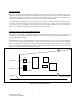
OUTPUT POWER
After all of the amplification and filtering is completed, a sample of the signal is measured and the output power is
predicted. This information is fed back to the Digital section and a Power Control voltage is generated and fed to the
input section attenuators to reduce the power if needed. This comprises the power control loop. Its response is slow
compared to the CDMA closed loop power control, so it will not interfere with the system.
The output power of both RF links is set at the factory to be nominally +23 dBm. As the input signal increases to a
level which, when added to the gain produces an output power larger than the set point, the power control loop takes
over to reduce the gain accordingly. This insures that under all input signal conditions below the maximum input
signal level (-35 dBm), that the integrity of the CDMA spectrum be maintained.
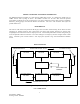
CHANNEL AND ATTENUATION PROGRAMMING
Programming of the 48660 is accomplished either by DIP Switch Programming of the unit, or remotely via a
computer (See Remote Programming Manual TBD). This section addresses the DIP Switch Programming of the
Channel and Attenuator Settings.
The DIP Switches (S1) are on the Digital Board located just inside the shroud. They can be accessed by opening the
shroud and with a pointed instrument such as a pencil or pen, can be set to certain values to set the frequency
(Channel Number) and the Attenuation Settings for the Down Link and Up Link, see Figure XX. Care should be
taken when closing the 48660 Intelli BDA shroud to disengage the latching mechanism located at the back of the
shroud. Forcing the shroud closed will damage the shroud.
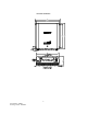
Load Button
DIP Switches
Front Panel
Figure X.X Location of DIP Switch
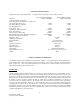
A7 MSB
A0 LSB
1
1
0
0
SW2
S1
Not Drawn to Scale