
User's Manual
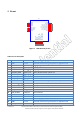

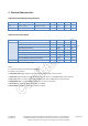
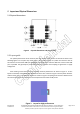
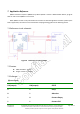
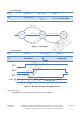
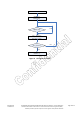
Table Of Contents

Rev1.4(4/23) Confidential and Proprietary ©2012-2014 by Quintic Corporation, not for distribution. Page 11 of 13
Confidential A Confidential Information contained herein is covered under Non-Disclosure Agreement (NDA).
Preliminary datasheet, Quintic Corporation reserves right to modify without notification
(b) State change:
GPIO Function timer cycle Remark
P03 State change
t1
t1>=1ms ;Falling edge
Sleep
Advertising
Connect
State Change
State Change State Change
10s Time out
Wait Master connect
Init
Figure 7 state change
(c) Data transmit
GPIO Function timer cycle Remark
P12 RX Wakeup
Falling edge
Data 1
P23
P24
UART_RX
Data 2
Data n
t2
P12
Figure 8 Waveform of module receiving UART data
NOTE: (1) T2>=1ms.
(2) RX Wakeup pin should keep low until one frame sent completed.