
QF4A512-DK Users Guide - Quickfilter


6) Running the Quickfilter development board’s QF4A512 using and external microcontroller:
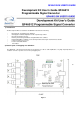
The QF4A512 – DK development board was designed for all signals to the QF4A512 to be tri-stated on power up through
either the USB power or externally connected power J7. The QF4A512 is ready for communication through the external
SPI connector J5. The correct chip select is Pin 7 QF4A512_CS. See Figure 3 above. No PC software is required for
this feature. Just plug the development board into a USB and start communicating with the QF4A512 through J5. It is
also possible to program the QF4A512 with Quickfilter Pro Software and then tri-state the controlling pins without losing
power so that all the external microcontroller needs to do is talk to the QF4A512. This control is done in Quickfilter Pro
Software.
7) Using an external clock source:
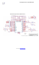
Since the crystal is lightly loaded, an external driving clock source can directly run the internal PLL. You do not need
to remove the 1 Meg resistor, crystal or 18 pF loading capacitors from the development board. Simply apply the
external clock source to Test Point TP22. Make sure to tell the Quickfilter software the external clock frequency used
when regenerating the QFP file.
Designer’s note – The allowable input range is 5 MHz to 200 MHz.
The clock input on Pin 22 to the phase lock loop is a 1.8 Volt level. Therefore the amplitude of
the incoming clock source should be 1.62 to 1.98 Volts Peak to peak. Since the input is AC
coupled, a DC offset can exist. The clock can be a sine wave, or square wave.
1
GND
TP22