
Users Manual


LTE Standard Module Series
EC200T Series Mini PCIe Hardware Design
EC200T_Series_Mini_PCIe_Hardware_Design 23 / 54
3.4.2. Airplane Mode
When the module enters airplane mode, the RF function will be disabled, and all AT commands related to
it will be inaccessible. For more details, please refer to Chapter 3.10.3.
3.5. Power Supply
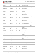
The following table shows pin definition of VCC_3V3 pins and ground pins.
Table 6: Definition of VCC_3V3 and GND Pins
The typical supply voltage of EC200T Series Mini PCIe is 3.3 V. In the 2G network, the input peak current
may reach 2.7 A during the transmitting time. Therefore, the power supply must be able to provide a rated
output current of 2.7 A at least, and a bypass capacitor of no less than 470 µF with low ESR should be
used to prevent the voltage from dropping. If the switching power supply is used to supply power to the
module, the power device and power supply routing traces of the switching power supply should be kept
away from the antennas as much as possible to prevent EMI interference.
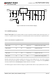
The following figure shows a reference design of power supply where R2 and R3 are 1% tolerance
resistors and C3 is a low-ESR capacitor.
Pin Name Pin No. I/O Power Domain Description
VCC_3V3 2, 39, 41, 52 PI 3.0 V–3.6 V Power supply for the module
GND
4, 9, 15, 18, 21,
26, 27, 29, 34, 35,
37, 40, 43, 50
Mini card ground