
Users Manual

Automotive Module Series
AG525R-GL QuecOpen
Hardware Design
AG525R-GL_QuecOpen_Hardware_Design 31 / 104
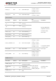
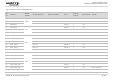
RGMII_RX_1 14 DI
RGMII receive data
bit 1
RGMII_CTL_RX 15 DI
RGMII receive
control
RGMII_RX_2 16 DI
RGMII receive data
bit 2
RGMII_RX_3 17 DI
RGMII receive data
bit 3
RGMII_CK_RX 19 DI RGMII receive clock
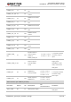
RGMII_TX_0 20 DO
RGMII transmit data
bit 0
RGMII_CTL_TX 21 DO
RGMII transmit
control
RGMII_TX_1 22 DO
RGMII transmit data
bit 1
RGMII_TX_2 23 DO
RGMII transmit data
bit 2
RGMII_CK_TX 24 DO
RGMII transmit
clock
RGMII_TX_3 25 DO
RGMII transmit data
bit 3
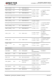
RGMII_PWR_
EN
27 DO
Enable external
LDO to supply
power to
RGMII_PWR_IN
V
OL
max = 0.45 V
V
OH
min = 1.35 V
1.8 V power domain.
If unused, keep it
open.
RGMII_PWR_IN 28 PI
Power input for
internal RGMII
circuit
1.8/2.5 V power
supply input.
If RGMII is not be
used, connect it to
VDD_EXT.
RGMII_INT 29 DI
RGMII PHY
interrupt output
V
IL
min = -0.3 V
V
IL
max = 0.63 V
V
IH
min = 1.17 V
V
IH
max = 2.1 V
1.8 V power domain.
If unused, keep
them open.
RGMII_RST 31 DO
Reset output for
RGMII PHY
V
OL
max = 0.45 V
V
OH
min = 1.35 V
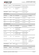
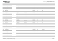
SDIO Interface (for eMMC by default)
Pin Name Pin No. I/O Description
DC
Characteristics
Comment
SDIO_VDD 60 PI SDIO power supply
connect it to
VDD_EXT.