
EVB User Guide V1.0
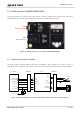
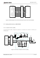
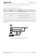
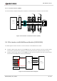
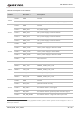
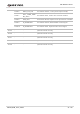
Table Of Contents
- Safety Information
- About the Document
- Contents
- Table Index
- Figure Index
- 1 Introduction
- 2 General Overview
- 3 Interface Application
- 3.1. Power Supply (J0202/J0601)
- 3.2. Switches, Button and Status Indicators
- 3.3. M.2 Interface (J0101)
- 3.4. USB Type-C Interface (J0601)
- 3.5. USB-TO-UART Interface (J0901/J0902)
- 3.6. (U)SIM Interfaces (J0701/J0702)
- 3.7. Audio Interfaces (J0801/J0802/J0803)
- 3.8 PCIe Interface to WLAN/Ethernet Module (J0501/J0502)
- 3.9. Antenna Interfaces
- 3.10. Test Points
- 4 Operation Procedures
- 5 Appendix References

5G Module Series
5G-M2_EVB_User_Guide 26 / 34
Table 8: Description of Test Points
3
Pin definitions might be different among applicable modules, please contact Quectel Technical Support in case of a
different pin definition.
RefDes
Pin Name
3
Description
J0102
J0102.1
GND
Ground
J0102.2
VCC
M.2 module (Pin 2, 4, 70, 72, 74) power supply
J1101
J1101.1
GND
Ground
J1101.2
PWR_5V0
5 V power supply
J1101.3
PWR_3V8
3.8 V power supply of DC-DC U0202
J1101.4
PWR_3V3
3.3 V power supply of DC-DC U0203
J1101.5
PWR_1V8
1.8 V power supply of DC-DC U0207
J1104
J1104.1
GND
Ground
J1104.2
PWR_1V95
1.95 V power supply of DC-DC U0206
J1104.3
PWR_1V35
1.35 V power supply of LDO U0205
J1104.4
PWR_0V95
0.95 V power supply of DC-DC U0204
J1104.5
NC
Not connected
J0902
J0902.1
GND
Ground
J0902.2
RXD_1V8
DEBUG_UART_RXD_1V8
J0902.3
TXD_1V8
DEBUG_UART_TXD_1V8
J0902.4
DTR_1V8
DEBUG_UART_DTR_1V8
J0902.5
RTS_1V8
DEBUG_UART_RTS_1V8
J1103
J1103.1
GND
Ground
J1103.2
RTS_RST
Quectel internal use only
J1103.3
M2_RST#
M.2 module Pin 67, reset signal
J1103.4
M2_DPR
M.2 module Pin 25, dynamic power reduction signal
J1103.5
WK_ON_WAN#
M.2 module Pin 23, a signal to wake up the host