
EVB User Guide V1.0
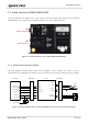
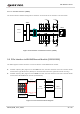
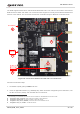
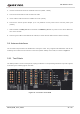
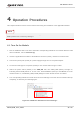
Table Of Contents
- Safety Information
- About the Document
- Contents
- Table Index
- Figure Index
- 1 Introduction
- 2 General Overview
- 3 Interface Application
- 3.1. Power Supply (J0202/J0601)
- 3.2. Switches, Button and Status Indicators
- 3.3. M.2 Interface (J0101)
- 3.4. USB Type-C Interface (J0601)
- 3.5. USB-TO-UART Interface (J0901/J0902)
- 3.6. (U)SIM Interfaces (J0701/J0702)
- 3.7. Audio Interfaces (J0801/J0802/J0803)
- 3.8 PCIe Interface to WLAN/Ethernet Module (J0501/J0502)
- 3.9. Antenna Interfaces
- 3.10. Test Points
- 4 Operation Procedures
- 5 Appendix References

5G Module Series
5G-M2_EVB_User_Guide 21 / 34
PCM_DIN
PCM_DOUT
PCM_SYNC
PCM_CLK
SPI_CS
SPI_CLK
LE9643
M.2 Module
PCLK
FS
DRA
DXA
CS#
DCLK
BTB CON
J0803
SPI_MOSI
SPI_MISO
INT#
RST#
DIN
DOUT
INT#
J0101
RST#
Figure 13: Block Diagram of the Connection Between the SLIC TE-A and the Module
3.7.2. Analog Audio Interfaces (J0801/J0802)
3.7.2.1. Earphone Interface (J0801)
The audio interface J0801 is designed for earphones. A schematic of the interface is shown by the
following figure.
SPK_L
MIC_N
MIC_P
33 pF
Close to Socket
Differential layout
10 pF
10 pF
33 pF
AGND
Codec
ALC5686
Close to Socket
ESD
ESD
Audio Jack
J0801
1
4
5
3
2
SPK_R
10 pF
33 pF
6
33 pF
AGND
10 pF
4.7 μF
BTB CON
J0803
AGND
AGND
AGND
AGND
ESD
1 μF
1 μF
Figure 14: Schematic of Earphone Interface (J0801)