
Product Info

Smart Module Series
SC200R Series Hardware Design
SC200R_Series_Hardware_Design 81 / 125
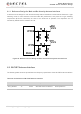
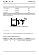
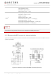
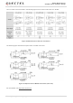
6.1.1. Reference Design for Main and Rx-diversity Antenna Interfaces
A reference circuit design for main and Rx-diversity antenna interfaces is shown below. Reserve a π-type
matching circuit for each antenna to achieve better RF performance, and place the π-type matching
components (R1/C1/C2, R2/C3/C4) as close to the antennas as possible. The capacitors are not
mounted by default and the resistors are 0 Ω.
Figure 29: Reference Circuit Design for Main and Rx-diversity Antenna Interfaces
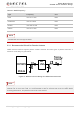
6.2. Wi-Fi/BT Antenna Interface
The following tables show the pin definition and frequency specification of the Wi-Fi/BT antenna interface.
Table 38: Pin Definition of Wi-Fi/BT Antenna Interface
Pin Name Pin No. I/O Description Comment
ANT_WIFI/BT 77 AI/AO Wi-Fi/BT antenna interface 50 Ω impedance