
Product Info

Smart Module Series
SC200R Series Hardware Design
SC200R_Series_Hardware_Design 28 / 125
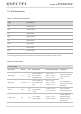
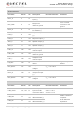
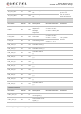
TP_I2C_SCL 47 OD
I2C clock signal of
TP
Externally pull them
up to 1.8 V.
Can be used for
other I2C devices.
TP_I2C_SDA 48 OD
I2C data signal of
TP
LCM Interface
Pin Name Pin No. I/O Description DC Characteristics
Comment
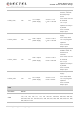
PWM 29 DO
PWM output which
adjusts the
backlight
brightness
V
OL
max = 0.45 V
V
OH
max = VBAT_BB
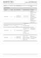
LCD_RST 49 DO
LCD reset
V
OL
max = 0.45 V
V
OH
min = 1.35 V
1.8 V power
domain.
LCD_TE 50 DI LCD tearing effect
V
IL
max = 0.63 V
V
IH
min = 1.17 V
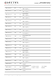
DSI_CLK_N 52 AO
LCD MIPI clock (-)
DSI_CLK_P 53 AO
LCD MIPI clock (+)
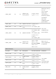
DSI_LN0_N 54 AO
LCD MIPI data 0
(-)
DSI_LN0_P 55 AO
LCD MIPI data 0
(+)
DSI_LN1_N 56 AO
LCD MIPI data 1
(-)
DSI_LN1_P 57 AO
LCD MIPI data 1
(+)
DSI_LN2_N 58 AO
LCD MIPI data 2
(-)
DSI_LN2_P 59 AO
LCD MIPI data 2
(+)
DSI_LN3_N 60 AO
LCD MIPI data 3
(-)
DSI_LN3_P 61 AO
LCD MIPI data 3
(+)
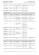
Camera Interfaces
Pin Name Pin No. I/O Description DC Characteristics
Comment
CSI1_CLK_N 63 AI
Camera MIPI
clock signal (-)
CSI1_CLK_P 64 AI
Camera MIPI clock
signal (+)