
Service Guide


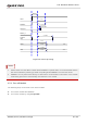
Table Of Contents
- Safety Information
- About the Document
- Contents
- Contents
- Table Index
- Figure Index
- 1 Introduction
- 2 Product Overview
- 3 Application Interfaces
- 3.1. General Description
- 3.2. Pin Assignment
- 3.3. Pin Description
- 3.4. Operating Modes
- 3.5. Power Saving
- 3.6. Power Supply
- 3.7. Turn on/Turn off/Reset
- 3.8. (U)SIM Interfaces
- 3.9. USB Interface
- 3.10. UART Interfaces
- 3.11. SPI Interface
- 3.12. I2C Interfaces
- 3.13. PCM Interface
- 3.14. Analog Audio Interfaces
- 3.15. LCD Interface
- 3.16. Matrix Keyboard Interface
- 3.17. SD Card Interface
- 3.18. WLAN Application Interface*
- 3.19. ADC Interfaces
- 3.20. Network Status Indication
- 3.21. STATUS
- 3.22. Behaviors of MAIN_RI
- 3.23. USB_BOOT Interface
- 4 Antenna Interfaces
- 5 Electrical Characteristics, Radio and Reliability
- 6 Mechanical Information
- 7 Storage, Manufacturing & Packaging
- 8 Appendix References

LTE Standard Module Series
EC200U_Series_Hardware_Design 31 / 94
3.6. Power Supply
3.6.1. Power Supply Pins
The module provides four VBAT pins for connection with the external power supply. There are two
separate voltage domains for VBAT.
⚫ Two VBAT_RF pins for module’s RF part.
⚫ Two VBAT_BB pins for module’s baseband part and RF part.
Table 9: VBAT and GND Pins
Pin Name
Pin No.
Description
Min.
Typ.
Max.
Unit
VBAT_RF
57, 58
Power supply for module’s
RF part
3.3
3.8
4.3
V
VBAT_BB
59, 60
Power supply for module‘s
baseband part and RF part
3.3
3.8
4.3
V
GND
8, 9, 19, 22, 36, 46, 48, 50–54, 56, 72, 76, 85–112
3.6.2. Voltage Stability Requirements
The power supply range of the module is from 3.3 V to 4.3 V. Please make sure that the input voltage will
never drop below 3.3 V. The following figure shows the voltage drop during burst transmission in 2G
network. The voltage drop will be less in 4G networks.
VBAT
Ripple
Drop
Burst
Transmission
Burst
Transmission
Figure 7: Power Supply Limits during Burst Transmission