
Service Guide


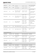


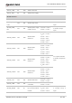

Table Of Contents
- Safety Information
- About the Document
- Contents
- Contents
- Table Index
- Figure Index
- 1 Introduction
- 2 Product Overview
- 3 Application Interfaces
- 3.1. General Description
- 3.2. Pin Assignment
- 3.3. Pin Description
- 3.4. Operating Modes
- 3.5. Power Saving
- 3.6. Power Supply
- 3.7. Turn on/Turn off/Reset
- 3.8. (U)SIM Interfaces
- 3.9. USB Interface
- 3.10. UART Interfaces
- 3.11. SPI Interface
- 3.12. I2C Interfaces
- 3.13. PCM Interface
- 3.14. Analog Audio Interfaces
- 3.15. LCD Interface
- 3.16. Matrix Keyboard Interface
- 3.17. SD Card Interface
- 3.18. WLAN Application Interface*
- 3.19. ADC Interfaces
- 3.20. Network Status Indication
- 3.21. STATUS
- 3.22. Behaviors of MAIN_RI
- 3.23. USB_BOOT Interface
- 4 Antenna Interfaces
- 5 Electrical Characteristics, Radio and Reliability
- 6 Mechanical Information
- 7 Storage, Manufacturing & Packaging
- 8 Appendix References

LTE Standard Module Series
EC200U_Series_Hardware_Design 22 / 94
PCM_DIN
24
DI
PCM data input
V
IL
min = -0.3 V
V
IL
max = 0.6 V
V
IH
min = 1.26 V
V
IH
max = 2.0 V
1.8 V power domain.
If unused, keep it
open.
PCM_DOUT
25
DO
PCM data output
V
OL
max = 0.45 V
V
OH
min = 1.35 V
PCM_SYNC
26
DI
PCM data frame
sync
V
IL
min = -0.3 V
V
IL
max = 0.6 V
V
IH
min = 1.26 V
V
IH
max = 2.0 V
1.8 V power domain.
If unused, keep it
open. The PCM
function only
supports slave
mode, not master
mode.
PCM_CLK
27
DI
PCM clock
V
IL
min = -0.3 V
V
IL
max = 0.6 V
V
IH
min = 1.26 V
V
IH
max = 2.0 V
SPI Interface
Pin Name
Pin No.
I/O
Description
DC Characteristics
Comment
SPI_CS
37
DO
SPI chip select
V
OL
max = 0.45 V
V
OH
min = 1.35 V
If you use a module
model that supports
GNSS function, the
SPI function of Pin
37–40 cannot be
used and needs to
be left unconnected.
SPI_MOSI
38
DO
SPI master mode
output
V
OL
max = 0.45 V
V
OH
min = 1.35 V
SPI_MISO
39
DI
SPI master mode
input
SPI_CLK
40
DO
SPI clock
V
OL
max = 0.45 V
V
OH
min = 1.35 V
LCD Interface
Pin Name
Pin No.
I/O
Description
DC Characteristics
Comment
LCD_FMARK
119
DI
LCD frame
synchronization
V
IL
min = -0.3 V
V
IL
max = 0.6 V
V
IH
min = 1.26 V
V
IH
max = 2.0 V
1.8 V power domain.
If unused, keep them
open.
LCD_RSTB
120
DO
LCD reset
V
OL
max = 0.45 V
V
OH
min = 1.35 V
LCD_SEL
121
-
Reserved
-
LCD_CS
122
DO
LCD chip select
V
OL
max = 0.45 V
V
OH
min = 1.35 V
LCD_CLK
123
DO
LCD clock
V
OL
max = 0.45 V
V
OH
min = 1.35 V
LCD_SDC
124
DO
LCD register
selection
V
OL
max = 0.45 V
V
OH
min = 1.35 V
LCD_SI/O
125
DIO
LCD data
V
IL
min = -0.3 V
V
IL
max = 0.6 V
V
IH
min = 1.26 V
V
IH
max = 2.0 V
ISINK
140
PI
Sink current input.
Imax = 200 mA
It is driven by the