
Service Guide


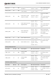


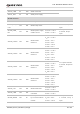

Table Of Contents
- Safety Information
- About the Document
- Contents
- Contents
- Table Index
- Figure Index
- 1 Introduction
- 2 Product Overview
- 3 Application Interfaces
- 3.1. General Description
- 3.2. Pin Assignment
- 3.3. Pin Description
- 3.4. Operating Modes
- 3.5. Power Saving
- 3.6. Power Supply
- 3.7. Turn on/Turn off/Reset
- 3.8. (U)SIM Interfaces
- 3.9. USB Interface
- 3.10. UART Interfaces
- 3.11. SPI Interface
- 3.12. I2C Interfaces
- 3.13. PCM Interface
- 3.14. Analog Audio Interfaces
- 3.15. LCD Interface
- 3.16. Matrix Keyboard Interface
- 3.17. SD Card Interface
- 3.18. WLAN Application Interface*
- 3.19. ADC Interfaces
- 3.20. Network Status Indication
- 3.21. STATUS
- 3.22. Behaviors of MAIN_RI
- 3.23. USB_BOOT Interface
- 4 Antenna Interfaces
- 5 Electrical Characteristics, Radio and Reliability
- 6 Mechanical Information
- 7 Storage, Manufacturing & Packaging
- 8 Appendix References

LTE Standard Module Series
EC200U_Series_Hardware_Design 16 / 94
3.3. Pin Description
The following tables show the pin definition of EC200U series module.
Table 6: I/O Parameters Definition
Type
Description
AI
Analog Input
AO
Analog Output
AIO
Analog Input/Output
DI
Digital Input
DO
Digital Output
DIO
Digital Input/Output
OD
Open Drain
PI
Power Input
PO
Power Output
Table 7: Pin Description
Power Supply
Pin Name
Pin No.
I/O
Description
DC Characteristics
Comment
VBAT_BB
59, 60
PI
Power supply for
module’s
baseband part
and RF part
Vmax = 4.3 V
Vmin = 3.3 V
Vnom = 3.8 V
It must be provided
with sufficient current
up to 1.5 A.
VBAT_RF
57, 58
PI
Power supply for
module’s RF part
Vmax = 4.3 V
Vmin = 3.3 V
Vnom = 3.8 V
It must be provided
with sufficient current
up to 2 A.
GND
8, 9, 19, 22, 36, 46, 48, 50–54, 56, 72, 76, 85–112
Module Output Power
Pin Name
Pin No.
I/O
Description
DC Characteristics
Comment