
Product Info


5G Module Series
RM500Q-AE&RM502Q-AE Hardware Design
RM500Q-AE&RM502Q-AE_Hardware_Design 59 / 83
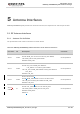
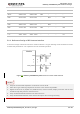
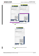
Figure 3031: Coplanar Waveguide Design on a 4-layer PCB (Layer 4 as Reference Ground)
To ensure RF performance and reliability, the following principles should be complied with in RF layout
design:
⚫ Use an impedance simulation tool to accurately control the characteristic impedance of RF traces to
50 Ω.
⚫ The GND pins adjacent to RF pins should not be designed as thermal relief pads, and should be fully
connected to ground.
⚫ The distance between the RF pins and the RF connector should be as short as possible, and all the
right-angle traces should be changed to curved ones. The recommended trace angle is 135°.
⚫ There should be clearance under the signal pin of the antenna connector or solder joint.
⚫ The reference ground of RF traces should be complete. Meanwhile, adding some ground vias around
RF traces and the reference ground could help to improve RF performance. The distance between
the ground vias and RF traces should be no less than two times the width of RF signal traces (2 × W).
⚫ Keep RF traces away from interference sources, and avoid intersection and paralleling between
traces on adjacent layers.
For more details about RF layout, see document [4].
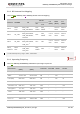
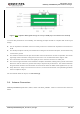
5.4. Antenna Connectors
RM500Q-AE&RM502Q-AE ANT0, ANT1, ANT2 and ANT3_GNSSL1 antenna connectors are shown as
below.