
Product Info


5G Module Series
RM500Q-AE&RM502Q-AE Hardware Design
RM500Q-AE&RM502Q-AE_Hardware_Design 38 / 83
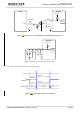
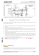
Host Module
USB_DM
USB_DP
USB_SS_RX_P
USB_SS_RX_M
USB_SS_TX_P
USB_SS_TX_M
BB
USB_DM
USB_DP
USB_SS_RX_P
USB_SS_RX_M
USB_SS_TX_P
USB_SS_TX_M
9
7
37
35
31
29
ESD
Test Points
Minimize these stubs in PCB layout.
C5 220 nF
C6 220 nF
C1 220 nF
C2 220 nF
R1 0Ω
R2 0Ω
R3 NM-0Ω
R4 NM-0Ω
Figure 16: Reference Circuit of USB 3.1 & 2.0 Interface
AC coupling capacitors C5 and C6 must be placed close to the host and close to each other. C1 and C2
have been integrated inside the module, so do not place these two capacitors on customers’ schematic
and PCB. In order tTo ensure the signal integrity of USB 2.0 data traces, R1, R2, R3 and R4 must be
placed close to the module, and the stubs must be minimized in PCB layout.
You should follow the principles below when designing for the USB interface to meet USB 3.1 and 2.0
specifications:
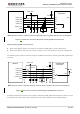
⚫ Route the USB signal traces as differential pairs with ground surrounded. The impedance of
differential trace of USB 2.0 and 3.1 is 90 Ω.
⚫ For USB 2.0 signal traces, the trace length should be less than 120 mm, and the differential data pair
matching should be less than 2 mm. For USB 3.1 signal traces, length matching of each differential
data pair (Tx/Rx) should be less than 0.7 mm, while the matching between Tx and Rx should be less
than 10 mm.
⚫ Do not route signal traces under crystals, oscillators, magnetic devices, PCIe and RF signal traces.
Route the USB differential traces in inner-layer of the PCB, and surround the traces with ground on
that layer and with ground planes above and below.
⚫ Junction capacitance of the ESD protection device might cause influences on USB data lines, so you
should pay attention to the selection of the device. Typically, the stray capacitance should be less
than 1.0 pF for USB 2.0, and less than 0.15 pF for USB 3.1.
⚫ Keep the ESD protection devices as close to the USB connector as possible.
⚫ If possible, reserve 0 Ω resistors on USB_DP and USB_DM lines respectively.