
Product Info

5G Module Series
RM500Q-AE&RM502Q-AE Hardware Design
RM500Q-AE&RM502Q-AE_Hardware_Design 28 / 83
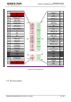
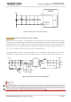
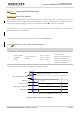
Module
PMU
2, 4, 70, 72, 74
C1
100 μF
D1
5.1 V
3, 5, 11, 27,
33, 39, 45,
51, 57, 71,
73
VCC
VCC
GND
C5
10 pF
C4
33 pF
C3
100 nF
C2
1 μF
+
Figure 4: Reference Circuit of VCC Pins
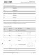
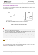
3.3.2.3.4.2. Reference Design for Power Supply
Power design for the module is very important, as the performance of the module largely depends on the
power source. The power supply is capable of providing a sufficient current of at least 3 A. If the voltage
drop between the input and output is not too high, it is suggested that an LDO is used to supply power for
the module. If there is a big voltage difference between the input source and the desired output (VCC =
3.7 V Typ.), a buck DC-DC converter is preferred as the power supply.
The following figure shows a reference design for +5 V input power source based on the DC-DC
TPS54319. The typical output of the power supply is about 3.7 V and the maximum load current is 3 A.
D1
TVS
PWR_IN
C8
220 μF
C11
10 pF
C10
33 pF
C9
100 nF
+
R1
205k
U1
Q1
NPN
R8
47k
R7
4.7k
PWR_EN
R4
182k
PWR_OUT
L1
1.5 μH
TPS54319
VIN
VIN
VIN
EN
VSNS
COMP
RT/CLK
SS
PH
PH
PH
BOOT
PWRGD
GND
GND
AGND
VFB
R5
330k 1%
R6
100k 1%
C6
100 nF
EP
17
R2
80.6k
C7
10 nF
R3
10k
C4
10 nF
C5
NM
VFB
C2
100 nF
C3
33 pF
C1
470 μF
+
Figure 5: Reference Design of Power Supply
To avoid damages to the internal flash, please do not switch off the power supply directly when the
module is working. It is suggested that the power supply can be cut off after the module is powered off by
pulling down the FULL_CARD_POWER_OFF# pin for more than 10 ss.
NOTE