
Product Info


5G Module Series
RM500Q-AE&RM502Q-AE Hardware Design
RM500Q-AE&RM502Q-AE_Hardware_Design 53 / 83
5.1.4. Reference Design of RF Antenna Interface
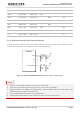
A reference design of antenna interface is shown as below. A π-type matching circuit should be reserved
for better RF performance. The capacitors are not mounted by default.
Module
ANT3_GNSSL1
ANT0
R1 0Ω
R4 0Ω
C1
NM
C2
NM
C8
NM
C7
NM
Figure 26: RM500Q-AE&RM502Q-AE Reference Circuit of RF Antenna
1. Keep the characteristic impedance for antenna trace as 50 Ω.
2. Place the π-type matching components as close to the antenna as possible.
3. Digital circuits such as (U)SIM card, USB interface, camera module, display connector and SD card
should be kept away from the antenna traces.
4. Keep 75 dB PCB isolation between two antenna traces.
5. Keep 15 dB isolation between each antenna to improve the receiving sensitivity.
B26
814–849
859–894
B26
–
–
–
WCS
2305–2315
2350–2360
B30
–
–
–
B38
2570–2620
2570–2620
–
B38
–
n38
B41/B41-XGP
2496–2690
2496–2690
–
B41
–
n41
B48
3550–3700
3550–3700
–
B48
–
-
B66
1710–1780
2110–2200
B66
–
–
n66
B71
663–698
617–652
B71
–
–
n71
n77
3300–4200
3300–4200
–
–
–
n77
NOTES