
Product Info


5G Module Series
RM500Q-AE&RM502Q-AE Hardware Design
RM500Q-AE&RM502Q-AE_Hardware_Design 36 / 83
3.9. PCIe Interface
RM500Q-AE&RM502Q-AE modules provide one integrated PCIe (Peripheral Component Interconnect
Express) interface which complies with the PCI Express Base Specification, Revision 3.0 and supports up
to 8 Gbps per lane.
⚫ PCI Express Base Specification Revision 3.0 compliant
⚫ Data rate up to 8 Gbps per lane
The following table shows the pin definition of PCIe interface.
Table 11: Pin Definition of PCIe Interface
3.9.1. PCIe Operating Mode
RM500Q-AE&RM502Q-AE supports endpoint (EP) mode and root complex (RC) mode. In EP mode, the
module is configured as a PCIe EP device. In RC mode, the module is configured as a PCIe root complex.
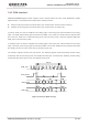
The following figure shows a reference circuit for the PCIe interface.
Pin No.
Pin Name
I/O
Description
Comment
55
PCIE_REFCLK_P
AI/AO
PCIe reference clock (+)
100 MHz. Require differential
impedance of 85 Ω
53
PCIE_REFCLK_M
AI/AO
PCIe reference clock (-)
49
PCIE_RX_P
AI
PCIe receive (+)
Require differential impedance
of 85 Ω
47
PCIE_RX_M
AI
PCIe receive (-)
43
PCIE_TX_P
AO
PCIe transmit (+)
Require differential impedance
of 85 Ω
41
PCIE_TX_M
AO
PCIe transmit (-)
50
PCIE_RST_N
DI
PCIe reset.
Open drain
Active LOW.
52
PCIE_CLKREQ_N
DO
PCIe clock request.
Open drain
Active LOW.
54
PCIE_WAKE_N
DO
PCIe wake up
Open drain
Active LOW.