
Product Info


LPWA Module Series
BG95 Hardware Design
BG95_Hardware_Design 57 / 88
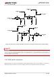
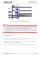
Table 23: Pin Definition of ADC Interface
Pin Name Pin No. I/O Description Comment
ADC0 24 AI General-purpose ADC interface
ADC0 and ADC1
cannot be used
simultaneously.
ADC1 2 AI General-purpose ADC interface
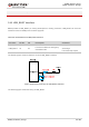
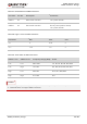
The following table describes the characteristics of ADC interfaces.
Table 24: Characteristics of ADC Interfaces
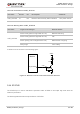
1. ADC input voltage must not exceed 1.8 V.
2. It is prohibited to supply any voltage to ADC pin when VBAT is removed.
3. It is recommended to use resistor divider circuit for ADC application, and the divider resistor accuracy
should be no less than 1%.
4. ADC0 and ADC1 cannot be used simultaneously, as ADC1 is connected directly to ADC0 inside the
module.
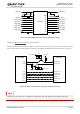
3.18. GPIO Interfaces*
The module provides nine general-purpose input and output (GPIO) interfaces. AT+QCFG="gpio"*
command can be used to configure the status of GPIO pins. For more details about the AT command,
please refer to document [2].
Parameter Min. Typ. Max. Unit
Voltage Range 0.1 1.8 V
Resolution (LSB) 64.979 μV
Analog Bandwidth 500 kHz
Sample Clock 4.8 MHz
Input Resistance 10 MΩ
NOTES