
Product Info


LPWA Module Series
BG95 Hardware Design
BG95_Hardware_Design 52 / 88
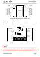
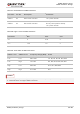
Table 17: Pin Definition of PCM and I2C Interfaces
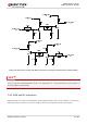
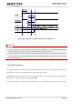
The following figure shows a reference design of PCM and I2C interfaces with an external codec IC.
PCM_DIN
PCM_SYNC
PCM_CLK
I2C_SCL
I2C_SDA
Module
1.8V
4.7K
4.7K
BCLK
WCLK
ADC
SCL
SDA
BIAS
MICBIAS
INP
INN
LOUTP
LOUTN
Codec
PCM_DOUT
DAC
Figure 20: Reference Circuit of PCM Application with Audio Codec
“*” means under development.
3.13. Network Status Indication
BG95 provides one network status indication pin: NET_STATUS. The pin is used to drive a network
status indication LED. The following tables describe the pin definition and logic level changes of
NET_STATUS in different network activity status.
Pin Name Pin No. I/O Description Comment
PCM_CLK 4 DO
PCM clock 1.8 V power domain.
PCM_SYNC 5 DO PCM data frame sync 1.8 V power domain.
PCM_DIN 6 DI PCM data input 1.8 V power domain.
PCM_DOUT 7 DO PCM data output
1.8 V power domain.
I2C_SCL 40 OD
I2C serial clock (for external
codec)
Require external pull-up to 1.8 V.
I2C_SDA 41 OD
I2C serial data (for external
codec)
Require external pull-up to 1.8 V.
NOTE