
Product Info


LPWA Module Series
BG95 Hardware Design
BG95_Hardware_Design 32 / 88
1. For every VBAT transition/re-insertion from 0 V, the minimum power supply voltage should be higher
than 2.7 V. After the module starts up normally, the minimum safety voltage is 2.6 V. In order to
ensure full-function mode, the minimum power supply voltage should be higher than 2.8 V.
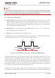
2. PWRKEY output voltage is 1.5 V because of the voltage drop inside the Qualcomm chipset. Due to
platform limitations, the chipset has integrated the reset function into PWRKEY. Therefore, PWRKEY
should never be pulled down to GND permanently.
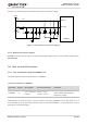
3. RESET_N is connected directly to PWRKEY inside the module.
4. ADC0 and ADC1 cannot be used simultaneously, as ADC1 is connected directly to ADC0 inside the
module. The module supports use of only one ADC interface at a time: either ADC0 or ADC1.
5. When PSM is enabled, the function of PSM_IND pin will be activated after the module is rebooted.
When PSM_IND is in high voltage level, the module is in normal operation state, when it is in low
voltage level, the module is in PSM. This function is under development currently.
6. GNSS_TXD (pin 27) and GRFC2 (pin 84) are BOOT_CONFIG pins. They should not be pulled up
before startup.
7. BG95-M4 does not support GRFC interfaces.
8. Keep all RESERVED pins and unused pins unconnected.
9. “*” means under development.
3.3. Operating Modes
The table below briefly summarizes the various operating modes of BG95.
Table 6: Overview of BG95 Operating Modes
Mode Details
Normal
Operation
Connected
Network has been connected. In this mode, the power consumption
may vary with the network setting and data transfer rate.
Idle
Software is active. The module remains registered on network, and it
is ready to send and receive data.
Extended Idle
Mode DRX
(e-I-DRX)
BG95 module and the network may negotiate over non-access stratum signaling the
use of e-I-DRX for reducing power consumption, while being available for mobile
terminating data and/or network originated procedures within a certain delay
dependent on the DRX cycle value.
Airplane Mode
AT+CFUN=4 or W_DISABLE#* pin can set the module into airplane mode. In this
case, RF function will be invalid.
Minimum
Functionality
AT+CFUN=0 can set the module into a minimum functionality mode without removing
the power supply. In this case, both RF function and (U)SIM card will be invalid.
NOTES